
Driving backboard, display panel and manufacturing method of driving backboard

A technology for driving backplanes and substrates, which is applied in the field of display panels and display panel production and driving backplanes, can solve the problems affecting the driving effect of the driving backplane, the high impedance of the second conductive layer, and the limitation, so as to improve the driving effect and reduce the The effect of self-impedance

Pending Publication Date: 2021-12-03
SHENZHEN CHINA STAR OPTOELECTRONICS SEMICON DISPLAY TECH CO LTD
View PDF3 Cites 0 Cited by
  • Summary
  • Abstract
  • Description
  • Claims
  • Application Information

AI Technical Summary

Problems solved by technology

In related technical solutions, the two conductive layers used to connect to the positive and negative electrodes of the external MicroLED chip in the drive backplane are formed by patterning the same metal layer, and are used to connect the second conductive layer to the negative electrode of the power supply. The range of layers that can be set is limited, and the film thickness of the second conductive layer is basically consistent with that of the first conductive layer, which leads to a higher impedance of the second conductive layer, which reduces the actual Vds and Vgs of the driving TFT, which in turn affects The driving effect of the driving backplane

Method used


Image

  • Driving backboard, display panel and manufacturing method of driving backboard
  • Driving backboard, display panel and manufacturing method of driving backboard
  • Driving backboard, display panel and manufacturing method of driving backboard

Examples


Embodiment 1

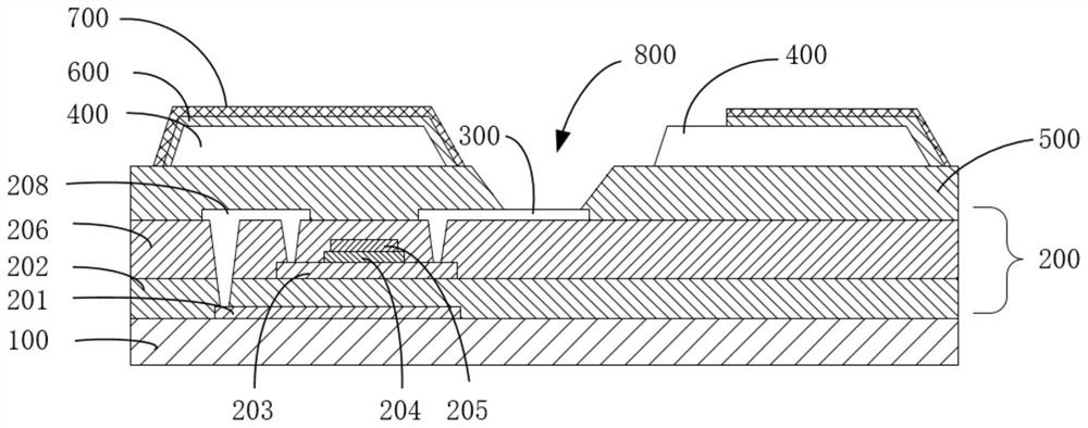
[0046] See figure 1 and combine figure 2 , the main body of this embodiment is a driving backplane, which is used to drive the light-emitting component 900. In this embodiment, the driving backplane includes:

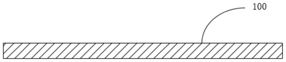
[0047] Substrate 100;

[0048] A thin film transistor layer 200, the thin film transistor layer 200 is disposed on the substrate 100, and the thin film transistor layer 200 includes a source and drain metal layer 208;

[0049] The first conductive layer 300 and the second conductive layer 400, the first conductive layer 300 and the second conductive layer 400 are arranged on the substrate 100, the first conductive layer 300 is electrically connected to the source and drain metal layer 208 connection, the first conductive layer 300 is used to electrically connect to the positive pole of the light emitting component 900, the second conductive layer 400 is used to electrically connect to the negative pole of the light emitting component 900, and the first conductive lay...

Embodiment 2

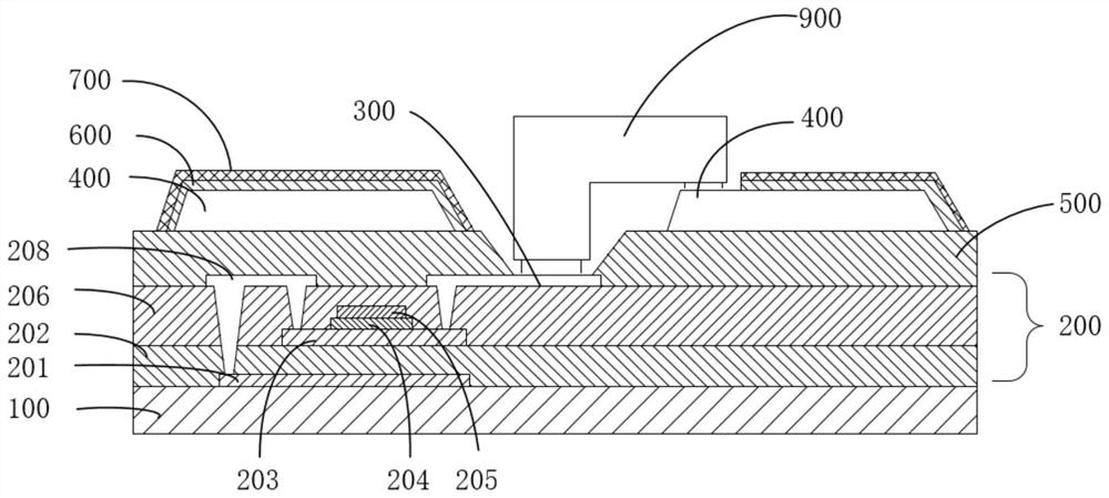
[0072] See figure 2 , this specific embodiment also provides a display panel as Example 2, the display panel provided in Example 2 includes a light-emitting component 900, and also includes a driving backplane as described in Example 1, and the light-emitting component 900 has A positive electrode connection end and a negative electrode connection end, the positive electrode connection end is electrically connected to the first conductive layer 300 , and the negative electrode connection end is electrically connected to the second conductive layer 400 .

[0073] Wherein, the above-mentioned light-emitting component 900 is specifically a MicroLED chip, and implementers can also replace the above-mentioned MicroLED chip with a MiniLED chip or an organic light-emitting diode.

Embodiment 3

[0075] Please combine Figure 3 to Figure 11 , this specific embodiment also provides a method for manufacturing a drive backplane, comprising the steps of:

[0076] providing a substrate 100;

[0077] A thin film transistor layer 200 is formed on the substrate 100, and a first conductive layer 300 for electrically connecting the anode of the light-emitting component 900 and a first conductive layer 300 for electrically connecting the cathode of the light-emitting component 900 are arranged on the thin film transistor. Two conductive layers 400, wherein the first conductive layer 300 and the second conductive layer 400 are arranged in different layers.

[0078] Wherein, on the substrate 100, a thin film transistor layer 200, a first conductive layer 300 for electrically connecting the anode of the light-emitting component 900, and a second conductive layer 400 for electrically connecting the cathode of the light-emitting component 900 are fabricated, specifically Include ste...


PUM


Abstract

The invention provides a driving backboard, a display panel and a manufacturing method of the driving backboard, and relates to the technical field of display devices. The driving backboard, the display panel and the driving backboard manufacturing method provided by the invention mainly improve the arrangement position of the conductive layer in the driving backboard. In the embodiment provided by the invention, the first conductive layer is used for being electrically connected with the positive electrode of the light-emitting part, and the second conductive layer is electrically connected with the negative electrode of the light-emitting part. According to the embodiment of the invention, the settable range of the second conductive layer and the thickness of the film layer are expanded, so that the second conductive layer can reduce the impedance of the second conductive layer by expanding the setting range of the second conductive layer and the thickness of the film layer, so that the driving effect of the driving backboard is improved.

Description

technical field [0001] The present invention relates to the technical field of display devices, in particular to a driving backplane, a display panel and a method for manufacturing the display panel. Background technique [0002] Micro LED display technology has the advantages of high brightness, good stability, and wide color gamut. It is widely recognized as the next generation of new display technology and is expected to be widely used in many fields. For the Micro LED current-driven display technology, it mainly establishes a connection with an external Micro LED chip through a conductive layer, thereby driving the Micro LED chip to emit light. In related technical solutions, the two conductive layers used to connect to the positive and negative electrodes of the external MicroLED chip in the drive backplane are formed by patterning the same metal layer, and are used to connect the second conductive layer to the negative electrode of the power supply. The range of layer...

Claims


Application Information

Patent Timeline
IPC IPC(8): H01L27/15H01L29/786H01L33/62
CPCH01L27/156H01L33/62H01L29/78633H01L2933/0066
Inventor 梅雪茹
Owner SHENZHEN CHINA STAR OPTOELECTRONICS SEMICON DISPLAY TECH CO LTD
Features
  • Generate Ideas
  • Intellectual Property
  • Life Sciences
  • Materials
  • Tech Scout
  • Unparalleled Data Quality
  • Higher Quality Content
  • 60% Fewer Hallucinations
Learn More