Defect detection method and device, electronic equipment and storage medium

A defect detection and defect technology, applied in the field of image processing, can solve the problems of high labor cost, time-consuming and laborious, etc., and achieve the effect of improving efficiency and accuracy

Pending Publication Date: 2021-12-07
创新奇智(青岛)科技有限公司
View PDF0 Cites 7 Cited by
  • Summary
  • Abstract
  • Description
  • Claims
  • Application Information

AI Technical Summary

Problems solved by technology

However, this detection method is time-consuming and labor-intensive, and the labor cost is high.

Method used


Image

  • Defect detection method and device, electronic equipment and storage medium
  • Defect detection method and device, electronic equipment and storage medium
  • Defect detection method and device, electronic equipment and storage medium

Examples


Embodiment Construction

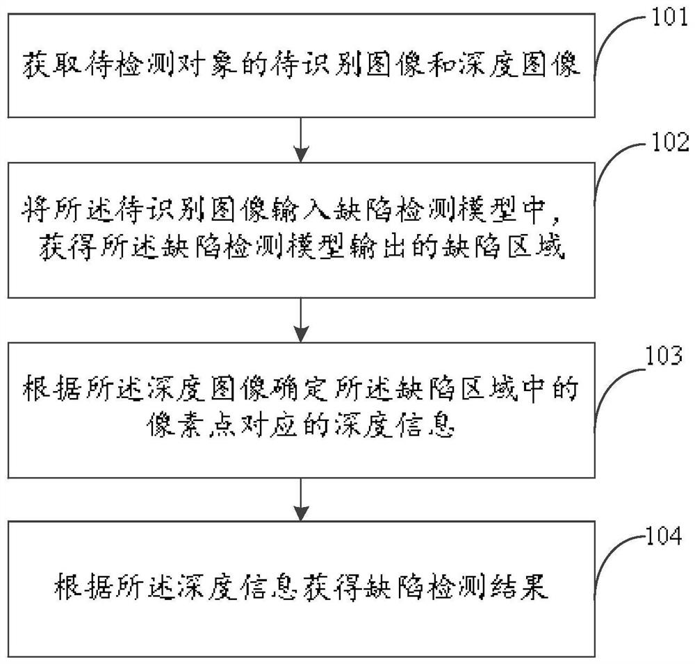
[0029] The inventors have found that by brushing soapy water on the casing of the electronic device to be tested and judging whether there are bubbles to determine whether the appearance defect is a functional defect, the efficiency of this method is low. Therefore, in order to solve this technical problem, the embodiment of the present application provides a defect detection method, which uses the defect detection model to determine the defect area from the image to be recognized, and combines the depth image to obtain the defect detection result. The result can be obtained by processing the collected images, and there is no need to brush soapy water on the casing, which greatly improves the efficiency of defect detection.

[0030] The defect detection method provided by the embodiment of the present application can be applied to the defect detection of the shell of electronic products, for example: the defect detection of the middle frame of the mobile phone, the defect detec...


PUM


Abstract

The invention provides a defect detection method and device, electronic equipment and a storage medium. The method comprises the steps of obtaining a to-be-recognized image and a depth image of a to-be-detected object, the pixel positions occupied by the to-be-detected object in the to-be-recognized image and the depth image being the same; inputting the to-be-recognized image into a defect detection model to obtain a defect area output by the defect detection model; determining depth information corresponding to pixel points in the defect area according to the depth image; and obtaining a defect detection result according to the depth information. According to the embodiment of the invention, image acquisition is carried out on the to-be-detected object, defect identification is carried out on the image, after the defect area is determined, the depth information is obtained by using the depth map corresponding to the defect area, and finally whether the defect is the target defect is determined according to the depth information. According to the embodiment of the invention, the defect detection is realized by processing the image, and the target defect is determined in combination with the depth information, so that the defect detection efficiency is improved.

Description

technical field [0001] The present application relates to the technical field of image processing, and in particular, to a defect detection method, device, electronic equipment, and storage medium. Background technique [0002] At present, the casings of electronic products need to undergo multiple quality inspections before they leave the factory. Taking the middle frame of a mobile phone as an example, it needs to be inspected for defects in its appearance before leaving the factory. [0003] The middle frame of the mobile phone will have defects due to the process when it is sealed. From the appearance of the image, the defects are in the shape of scratches, hollows, cracks, etc. These defects are defined as appearance defects. Appearance defects can be detected by brushing soapy water. If there are bubbles, it is defined as a functional defect. For the quality inspection of the middle frame gluing, the focus is on finding the functional defects in the appearance defect...

Claims


Application Information

Patent Timeline
Patent Type & Authority Applications(China)
IPC IPC(8): G06T7/00G06T7/11G06T7/50G06T7/73
CPCG06T7/0008G06T7/11G06T7/50G06T7/73G06T2207/10028
Inventor 张发恩李锴莹刁晓淳
Owner 创新奇智(青岛)科技有限公司
Why Eureka
Try Eureka