Probe structure for circuit board detection

A technology of circuit boards and probes, applied in the field of detection, can solve problems such as inability to quickly replace

Inactive Publication Date: 2021-12-10
怀化海红盛电子科技有限公司
View PDF0 Cites 2 Cited by
  • Summary
  • Abstract
  • Description
  • Claims
  • Application Information

AI Technical Summary

Problems solved by technology

[0002] The names of the circuit boards are: ceramic circuit board, alumina ceramic circuit board, aluminum nitride ceramic circuit board, circuit board, PCB board, aluminum substrate, high frequency board, thick copper board, impedance board, PCB, ultra-thin circuit board, ultra-thin Thin circuit board, printed circuit board, etc. The circuit board makes the circuit miniaturized and intuitive, and plays an important role in the mass production of fixed circuits and the optimization of the layout of electrical appliances. The circuit board can be called a printed circuit board or a printed circuit board. The circuit board is A highly reliable and excellent flexible printed circuit board made of polyimide or polyester film as the base material, featuring high wiring density, light weight, thin thickness and good bendability The birth and development of rigid-flex board and PCB gave birth to the new product of rigid-flex board. After the circuit board is produced, it is necessary to use probes to detect the circuit board. Traditional probes cannot be used quickly. Replacement to adapt to different circuit boards, so a probe structure for circuit board detection is proposed

Method used


Image

  • Probe structure for circuit board detection
  • Probe structure for circuit board detection
  • Probe structure for circuit board detection

Examples


Embodiment Construction

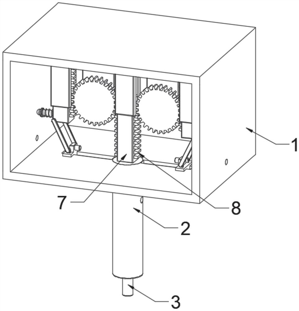
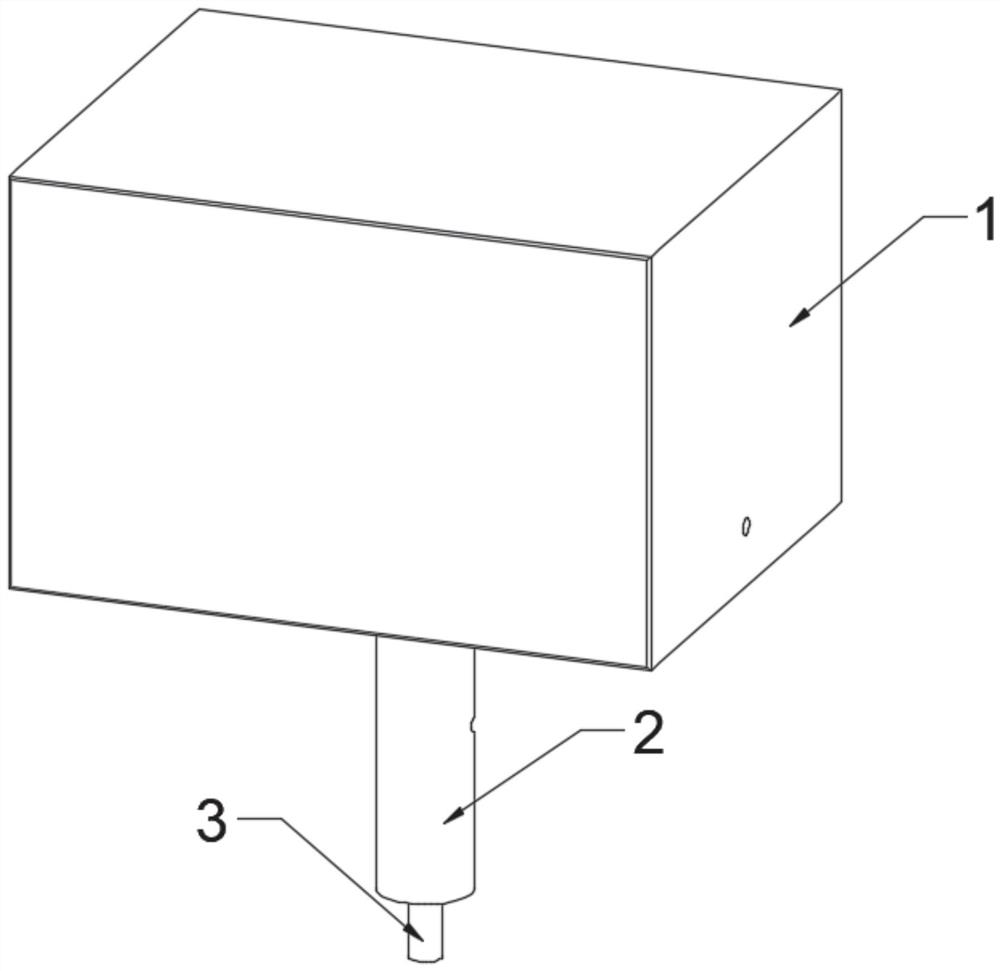
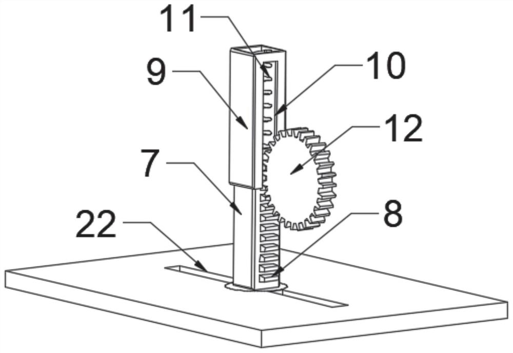
[0026] The following will clearly and completely describe the technical solutions in the embodiments of the present invention with reference to the accompanying drawings in the embodiments of the present invention. Obviously, the described embodiments are only some, not all, embodiments of the present invention. Based on the embodiments of the present invention, all other embodiments obtained by persons of ordinary skill in the art without making creative efforts belong to the protection scope of the present invention.

[0027] In addition, an element in the present invention is said to be "fixed" or "disposed on" another element, and it may be directly on another element or an intervening element may also exist. When an element is referred to as being "connected to" another element, it can be directly connected to the other element or intervening elements may also be present. The terms "vertical," "horizontal," "left," "right," and similar expressions are used herein for purp...


PUM


Abstract

The invention relates to a probe structure for circuit board detection. The probe structure for circuit board detection comprises: an assembly box with a hole in the bottom and a metal sleeve which is matched with the hole formed in the assembly box and is movably arranged on the assembly box, wherein the metal sleeve is also provided with a limiting hole, and the two sides of the assembly box are also provided with through holes; a limiting block, wherein the limiting block is matched with the limiting hole and is movably arranged in the assembly box; a probe assembly, wherein the probe assembly is movably arranged in the metal sleeve, and the probe assembly is used for detecting a circuit board; a clamping mechanism, wherein the clamping mechanism is connected with the limiting block, and the clamping mechanism drives the limiting block to enter the limiting hole when the metal sleeve moves towards the interior of the assembly box; elastic components, wherein the elastic components are movably and symmetrically arranged in the assembling box and are connected with the clamping mechanism; and a driving mechanism which is matched with the metal sleeve and is connected with the clamping mechanism.

Description

technical field [0001] The invention relates to the detection field, in particular to a probe structure for circuit board detection. Background technique [0002] The names of the circuit boards are: ceramic circuit board, alumina ceramic circuit board, aluminum nitride ceramic circuit board, circuit board, PCB board, aluminum substrate, high frequency board, thick copper board, impedance board, PCB, ultra-thin circuit board, ultra-thin Thin circuit board, printed circuit board, etc. The circuit board makes the circuit miniaturized and intuitive, and plays an important role in the mass production of fixed circuits and the optimization of the layout of electrical appliances. The circuit board can be called a printed circuit board or a printed circuit board. The circuit board is A highly reliable and excellent flexible printed circuit board made of polyimide or polyester film as the base material, featuring high wiring density, light weight, thin thickness and good bendability...

Claims


Application Information

Patent Timeline
Patent Type & Authority Applications(China)
IPC IPC(8): G01R1/067
CPCG01R1/06722G01R1/06733
Inventor 胡佳杰
Owner 怀化海红盛电子科技有限公司
Why Eureka
Try Eureka