Supercharge Your Innovation With Domain-Expert AI Agents!

Chip surface scratch defect detection method and device and computer equipment

A chip and scratch technology, used in computer parts, computing, character and pattern recognition, etc., can solve the problems of low detection accuracy and false detection, and achieve high detection accuracy, strong anti-interference, and superior detection performance. Effect

Pending Publication Date: 2021-12-10
CHINA ELECTRONICS PROD RELIABILITY & ENVIRONMENTAL TESTING RES INST
View PDF9 Cites 21 Cited by
  • Summary
  • Abstract
  • Description
  • Claims
  • Application Information

AI Technical Summary

Problems solved by technology

[0004] However, the existing computer image processing methods are usually based on threshold segmentation and morphology, which are prone to false detection and low detection accuracy.

Method used


Image

  • Chip surface scratch defect detection method and device and computer equipment
  • Chip surface scratch defect detection method and device and computer equipment
  • Chip surface scratch defect detection method and device and computer equipment

Examples


Embodiment Construction

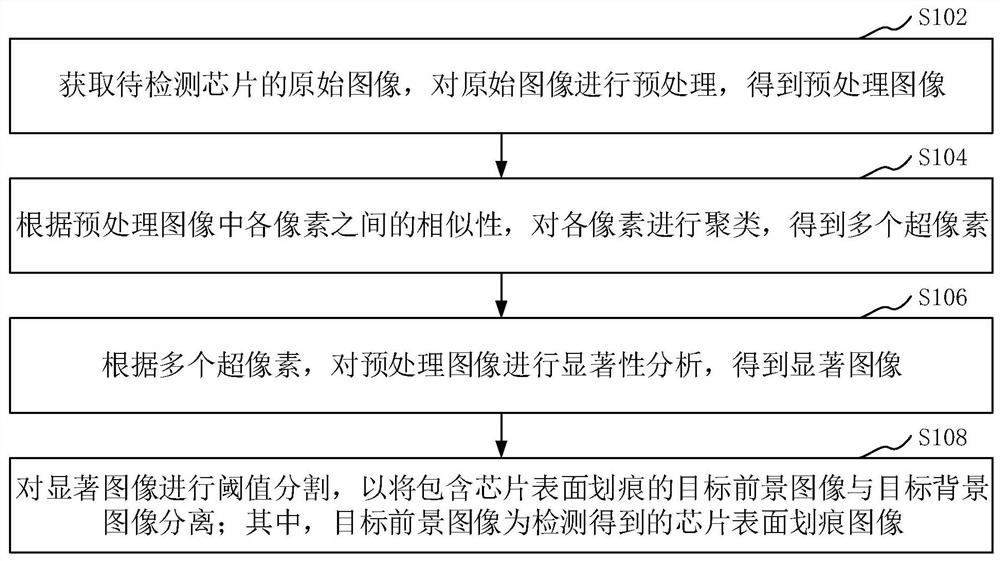
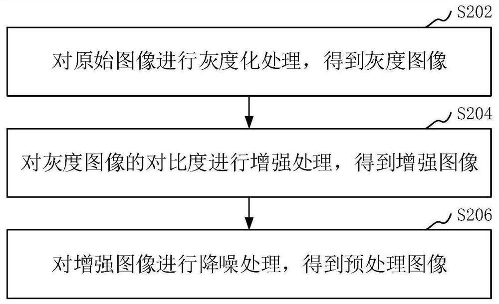
[0030] In order to make the purpose, technical solution and advantages of the present application clearer, the present application will be further described in detail below in conjunction with the accompanying drawings and embodiments. It should be understood that the specific embodiments described here are only used to explain the present application, and are not intended to limit the present application.

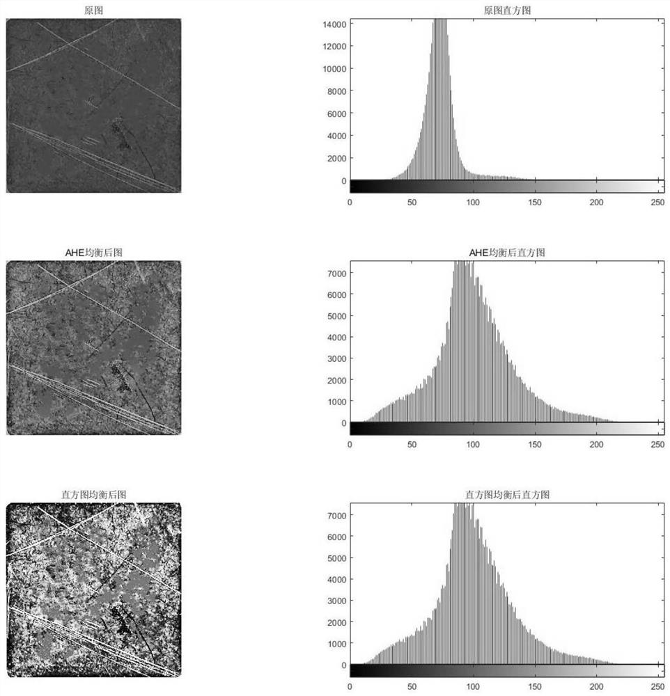
[0031]The current scratch defect detection method is mainly based on the method of threshold segmentation, and the chip defect image is binarized to separate the scratch position. However, since threshold segmentation only uses the threshold of the image and does not consider other image features, the image segmentation effect is poor for images with no obvious pixel differences between the target and the background (that is, low-contrast defect areas), and is susceptible to noise interference and illumination. conditional impact. However, the scratch area on the chip is ...


PUM


Abstract

The invention relates to a chip surface scratch defect detection method and device, computer equipment and a storage medium. The method comprises the following steps: acquiring an original image of a to-be-detected chip, and preprocessing the original image to obtain a preprocessed image; clustering pixels according to the similarity among the pixels in the preprocessed image to obtain a plurality of superpixels; performing significance analysis on the preprocessed image according to the plurality of superpixels to obtain a salient image; performing threshold segmentation on the salient image to separate a target foreground image containing chip surface scratches from a target background image, wherein the target foreground image is a chip surface scratch image obtained through detection. By adopting the method, the detection accuracy of scratches on the surface of a chip is high, and the robustness is strong.

Description

technical field [0001] The present application relates to the field of chip technology, and in particular to a detection method, device, computer equipment and storage medium for chip surface scratch defects. Background technique [0002] With the rapid development and widespread use of the modern electronics industry, the demand for chips continues to rise. However, chips are prone to some surface defects during production and transportation, which will affect their subsequent working performance. Traditional detection methods are mainly based on manual visual inspection, which not only has low detection efficiency and poor accuracy, but also is easily affected by human subjective factors, which makes it difficult to meet the actual detection needs of modern industries. [0003] As an important branch of artificial intelligence technology, computer vision can replace the human eye for detection and recognition, that is, to obtain images through visual modules (cameras, len...

Claims


Application Information

Patent Timeline
IPC IPC(8): G06T7/00G06T7/11G06T7/136G06T7/90G06T5/00G06K9/62
CPCG06T7/11G06T7/0004G06T7/136G06T7/90G06F18/23G06T5/70
Inventor 赵玥罗军王小强罗道军唐锐
Owner CHINA ELECTRONICS PROD RELIABILITY & ENVIRONMENTAL TESTING RES INST
Features
  • R&D
  • Intellectual Property
  • Life Sciences
  • Materials
  • Tech Scout
  • Unparalleled Data Quality
  • Higher Quality Content
  • 60% Fewer Hallucinations
Learn More