Three-dimensional memory and preparation method thereof

A memory, three-dimensional technology, applied in semiconductor/solid-state device manufacturing, capacitors, electric solid-state devices, etc., can solve the problem of affecting the connection performance of peripheral circuits and memory cell array circuits, affecting the formation of peripheral circuit layout, reducing the size of semiconductor structures, etc. problem, achieve the effect of optimizing electrical signal transmission performance, optimizing layout form, and simplifying manufacturing cost

Pending Publication Date: 2021-12-10
YANGTZE MEMORY TECH CO LTD
View PDF0 Cites 0 Cited by
  • Summary
  • Abstract
  • Description
  • Claims
  • Application Information

AI Technical Summary

Problems solved by technology

[0003] However, as the number of stacked layers in 3D NAND technology increases, the size of the semiconductor structure used to form the memory cell array decreases while achieving the same storage capacity
Correspondingly, the semiconductor structure with peripheral circuits tha

Method used


Image

  • Three-dimensional memory and preparation method thereof
  • Three-dimensional memory and preparation method thereof
  • Three-dimensional memory and preparation method thereof

Examples


Example Embodiment

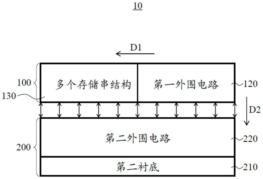
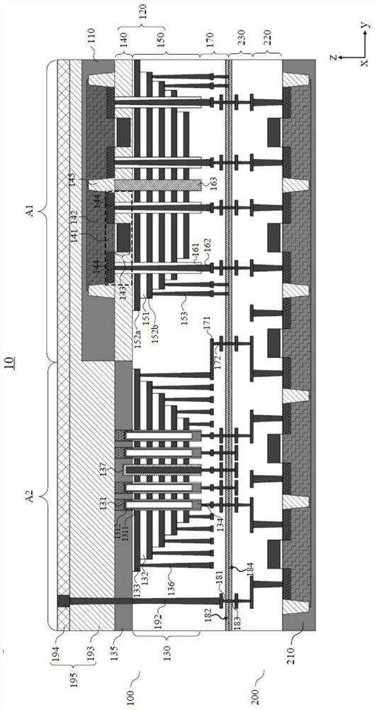
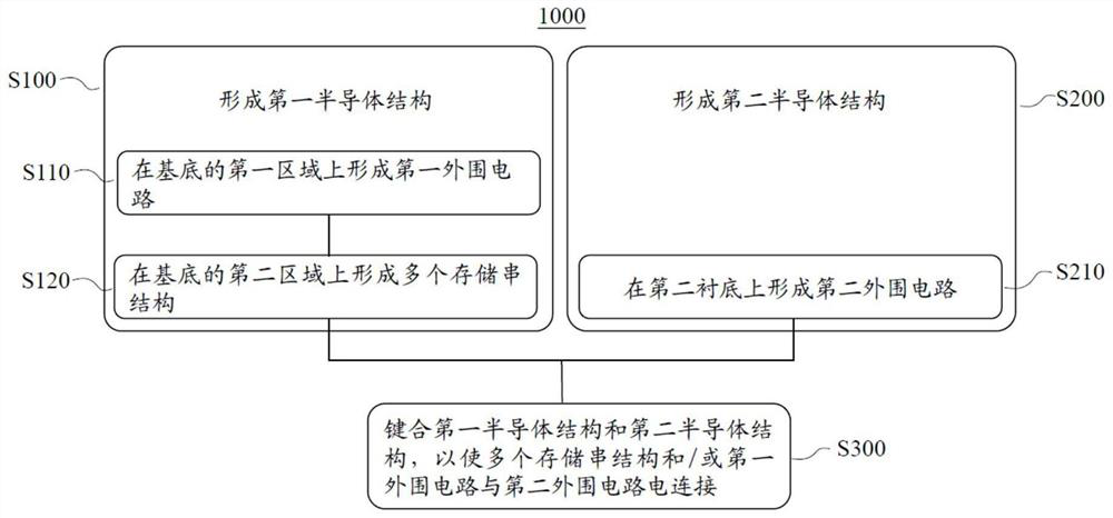
[0033] For a better understanding of the present application, various aspects of the present application will be described in more detail with reference to the accompanying drawings. It should be understood that these detailed descriptions are merely illustrative of exemplary embodiments of the present application and are not intended to limit the scope of the present application in any way.

[0034] The terminology used herein is for the purpose of describing particular example embodiments and is not intended to be limiting. When used in this specification, the terms "comprising", "comprising", "including" and / or "comprising" indicate the presence of stated features, integers, elements, parts and / or combinations thereof, but do not exclude The presence of one or more other features, integers, elements, components and / or combinations thereof.

[0035] This document is described with reference to schematic illustrations of exemplary embodiments. The exemplary embodiments disc...


PUM


Abstract

The invention provides a three-dimensional memory and a preparation method thereof. The three-dimensional memory comprises: a first semiconductor structure comprising a first peripheral circuit and a plurality of memory string structures which are distributed along a first direction; and a second semiconductor structure comprising a second substrate and a second peripheral circuit located on the second substrate. The first semiconductor structure and the second semiconductor structure are in bonding connection, so that the plurality of memory string structures and/or the first peripheral circuit are electrically connected with the second peripheral circuit. According to the three-dimensional memory and the preparation method thereof provided by the invention, the arrangement form of the peripheral circuit and the plurality of memory string structures can be optimized, and the electric signal transmission performance of the peripheral circuit and the plurality of memory string structures can be optimized.

Description

technical field [0001] The present application relates to the technical field of semiconductors, and more specifically, to a three-dimensional memory and a manufacturing method thereof. Background technique [0002] In a three-dimensional memory (3D NAND) based on the Xtacking architecture, peripheral circuits responsible for data I / O and memory cell operations are formed on the same substrate, and a memory cell array is formed on another substrate. After the two semiconductor structures are respectively prepared, the two semiconductor structures are bonded and connected to connect the memory cell array and the peripheral circuit. [0003] However, as the number of stacked layers of the 3D NAND technology increases, the size of the semiconductor structure used to form the memory cell array decreases accordingly while achieving the same storage capacity. Correspondingly, the semiconductor structure with peripheral circuits that is bonded to the semiconductor structure with m...

Claims


Application Information

Patent Timeline
IPC IPC(8): H01L27/11529H01L27/11531H01L49/02H01L21/8239
CPCH01L28/75H10B41/41H10B41/42
Inventor 陈亮
Owner YANGTZE MEMORY TECH CO LTD
Why Eureka
Try Eureka