Device and process method for controlling micro scratches on polished surface of silicon wafer

A technology for polishing silicon wafers and silicon wafers, which is applied in the direction of grinding/polishing safety devices, machine tools for surface polishing, manufacturing tools, etc. Chip surface micro scratches and other problems

Pending Publication Date: 2021-12-31
杭州中欣晶圆半导体股份有限公司
View PDF16 Cites 0 Cited by
  • Summary
  • Abstract
  • Description
  • Claims
  • Application Information

AI Technical Summary

Problems solved by technology

[0004] Aiming at the deficiencies of the prior art, the present invention provides a device and process method for controlling micro-scratches on the polished surface of silicon wafers, which solves the problem that the traditional method of polishing silicon wafers on the edge of circular silicon wafers cannot guarantee the polishing of all places on the entire flat edge. Uniformity, and the relative movement angle between the polishing cloth and the edge of the silicon wafer is not fixed, it is easy to cause irregular polishing scratches at various angles on the reference surface of the silicon wafer, and the edge of the silicon wafer is easy to adhere to particles during polishing, which is easy to The problem of micro-scratches on the surface of silicon wafers

Method used


Image

  • Device and process method for controlling micro scratches on polished surface of silicon wafer
  • Device and process method for controlling micro scratches on polished surface of silicon wafer
  • Device and process method for controlling micro scratches on polished surface of silicon wafer

Examples


Embodiment Construction

[0045] The following will clearly and completely describe the technical solutions in the embodiments of the present invention with reference to the accompanying drawings in the embodiments of the present invention. Obviously, the described embodiments are only some, not all, embodiments of the present invention. Based on the embodiments of the present invention, all other embodiments obtained by persons of ordinary skill in the art without making creative efforts belong to the protection scope of the present invention.

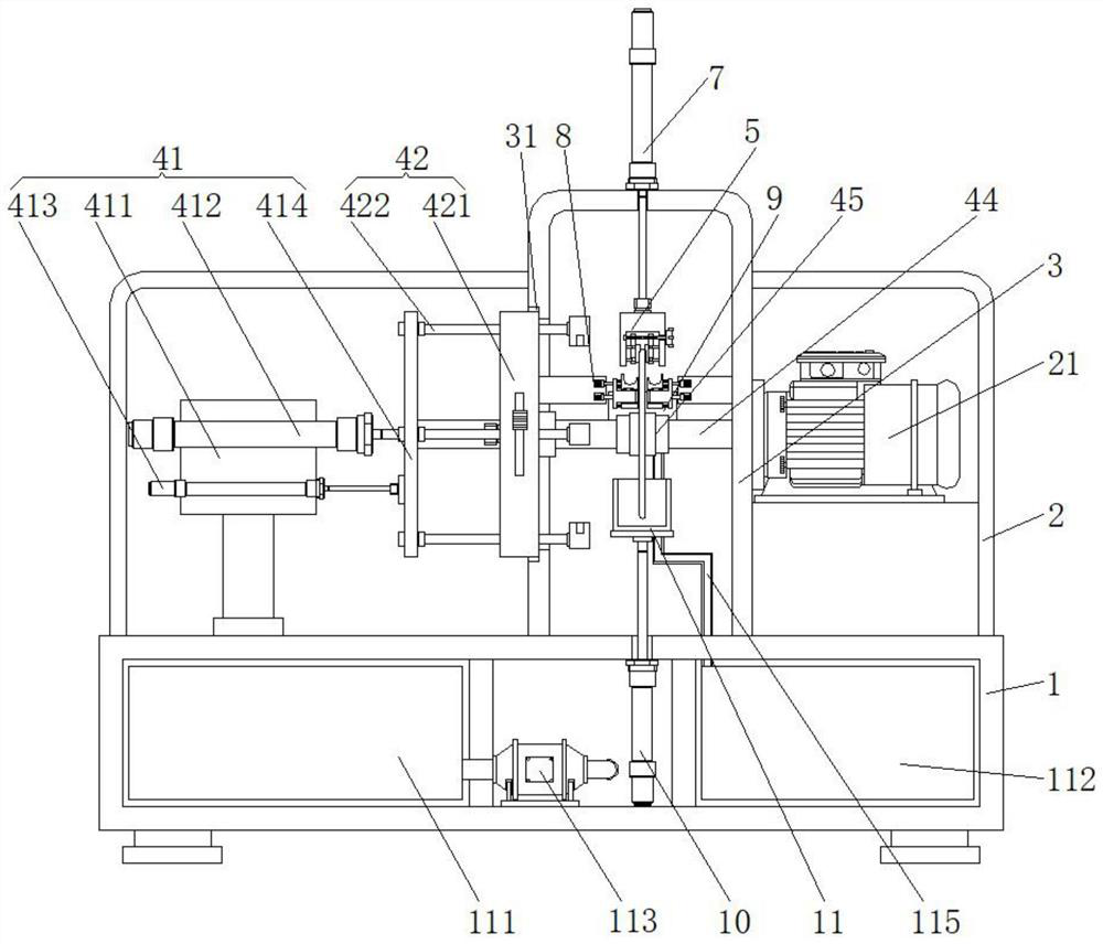
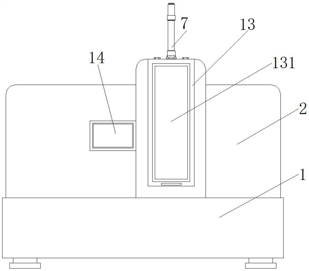
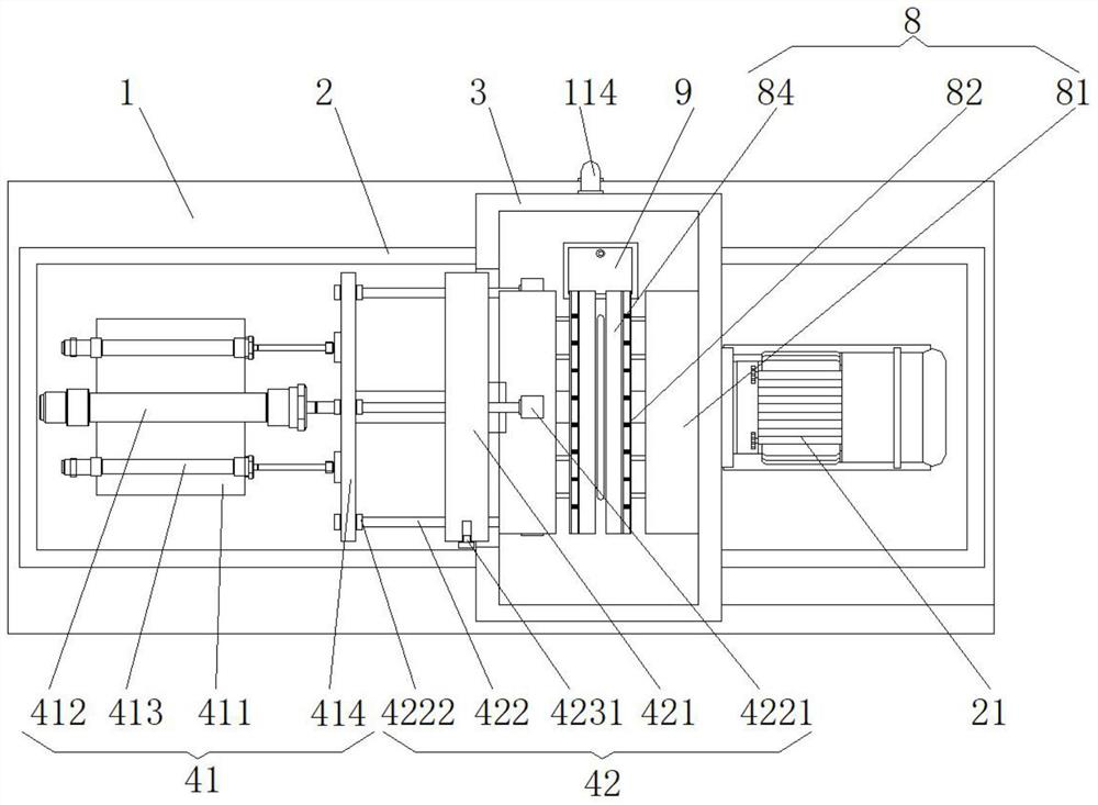
[0046] see Figure 1-7 , the present invention provides a technical solution: a device and a process method for controlling micro-scratches on the polished surface of a silicon wafer, comprising a base case 1 and an upper case 2, the middle part of the upper case 2 is connected in series with a polishing case 3, and the polishing case 3 The front side is hinged with a first cover door 13, and the middle part of the first cover door 13 is fixedly connected with...


PUM


Abstract

The invention discloses a device and a process method for controlling micro scratches on the polished surface of a silicon wafer. The device comprises a base box and an upper case, a grinding box is connected to the middle of the upper case in series, a penetrating opening is formed at the left side of the grinding box, and a positioning extrusion mechanism is arranged at the left side of an inner cavity of the upper case. The invention relates to the technical field of silicon wafer polishing. According to the device and the process method for controlling the micro scratches on the polished surface of the silicon wafer, a first electric push rod drives an edge polishing mechanism to move downwards, a screw rod and corner polishing stones rotate spirally, the corner polishing stones are clamped on the two sides of the round silicon wafer, the device and the process method are suitable for corner polishing of various round silicon wafers, and a water spraying head sprays water to the edge of the upper portion of the round silicon wafer; and a water draining rubber strip receives flushing ionized water sprayed out of the water spraying head, the water scraping rubber strip scrapes off grinding fluid adsorbed on the lower portion of the round silicon wafer, the situation that the polishing effect is affected due to impurity adsorption and long-time corrosion of the grinding fluid is avoided, a polishing block repairs the surface of the edge of the silicon wafer, and the micro scratches on the surface of the silicon wafer are better controlled.

Description

technical field [0001] The invention relates to the technical field of silicon wafer polishing, in particular to a device and a process method for controlling micro-scratches on the polished surface of silicon wafers. Background technique [0002] Silicon material is the main substrate material for the manufacture of VLSI. With the rapid development of the semiconductor industry, the precision requirements for substrate materials are getting higher and higher, especially for the edge state of silicon polished wafers. [0003] In the traditional method of polishing silicon wafers on the edge of circular silicon wafers, the uniformity of polishing on the entire flat edge cannot be guaranteed due to local contact, and the relative movement angle between the polishing cloth and the edge of the silicon wafer is not fixed, which is easy to make the silicon Irregular polishing scratches at various angles appear on the reference surface of the wafer, which reduces the smoothness of ...

Claims


Application Information

Patent Timeline
Patent Type & Authority Applications(China)
IPC IPC(8): B24B29/02B24B41/06B24B47/00B24B41/02B24B47/12B24B41/04B24B55/06B24B41/00B08B11/00H01L21/02
CPCB24B29/02B24B41/06B24B47/00B24B41/02B24B47/12B24B41/04B24B55/06B24B41/00B08B11/00H01L21/02013H01L21/02021H01L21/02052
Inventor 张森阳
Owner 杭州中欣晶圆半导体股份有限公司
Why Eureka
Try Eureka