Single-layer and multi-layer micro-nano structure pattern sample tracking device and method

A technology of micro-nano structure and tracking device, which is applied in the direction of measuring devices, instruments, scientific instruments, etc., can solve problems such as defocus, unusable, and poor quality of collected images, and achieve a wide range of applications

Pending Publication Date: 2022-01-07
SHANGHAI INST OF OPTICS & FINE MECHANICS CHINESE ACAD OF SCI
View PDF0 Cites 2 Cited by
  • Summary
  • Abstract
  • Description
  • Claims
  • Application Information

AI Technical Summary

Problems solved by technology

When detecting and reading single-layer and multi-layer micro-nano structure graphic samples, it is necessary to use an objective lens with a large magnification and a small depth of field, which is prone to defocus during the s

Method used


Image

  • Single-layer and multi-layer micro-nano structure pattern sample tracking device and method
  • Single-layer and multi-layer micro-nano structure pattern sample tracking device and method
  • Single-layer and multi-layer micro-nano structure pattern sample tracking device and method

Examples


Embodiment 1

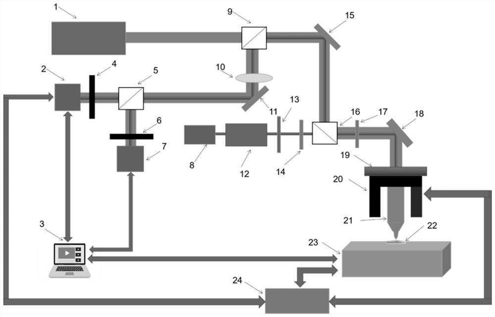
[0024] Such as figure 1 As shown, the single-layer and multi-layer micro-nano structure tracking device is characterized in that it includes an illumination module 1, a linear array CCD2, a computer 3, a first aperture 4, a light splitting element 5, a second aperture 6, an area array CCD7, Laser 8, beam splitting prism 9, imaging lens 10, third reflector 11, beam expander 12, attenuation plate 13, 1 / 2 wave plate 14, first reflector 15, polarization beam splitting prism 16, 1 / 4 wave plate 17 , second reflector 18, coarse motor 19, piezoelectric ceramics 20, objective lens 21, micro-nano structure pattern sample 22, displacement stage 23, controller 24;

[0025] The white light emitted by the lighting module 1 passes through the dichroic prism 9 and the first reflector 15 in sequence, and after being reflected by the polarizing dichroic prism 16, passes through the 1 / 4 wave plate 17, the second reflector 18, and the objective lens 21 to reach the micro-nano structure Graphic s...


PUM


Abstract

The invention relates to a single-layer and multi-layer micro-nano structure pattern sample tracking device and method. The device comprises an illumination module, a linear array CCD, a computer, a diaphragm, a beam splitter prism, an area array CCD, a laser, a light splitting element, an imaging lens, a reflector, a beam expander, an attenuation sheet, a 1/2 wave plate, a polarization splitting prism, a 1/4 wave plate and the like. The micro-nano structure pattern sample is placed on the displacement table, the surface of the micro-nano structure pattern sample is clearly imaged in the area array CCD through the coarse adjustment motor, the defocusing amount of the current position is obtained through laser spot diameter data collected by the linear array CCD, and the piezoelectric ceramic is controlled to automatically track in real time. The tiny change of the laser spot can be detected by using high-precision pixels in the linear array CCD, the laser spot is secondarily amplified through the objective lens and the imaging system, so that the change rate of the laser spot is increased, and the system sensitivity is high. According to the method, the out-of-focus distance is obtained by measuring the spot diameter at a high speed in real time through the linear array CCD instead of being judged through spot energy.

Description

technical field [0001] The invention relates to the field of high-speed tracking of single-layer and multi-layer micro-nano structure graphic samples, and is a high-speed, high-precision, high-sensitivity tracking control method based on laser spot diameter detection of defocus, which can be used for single-layer and multi-layer micro-nano structure graphics Automatic tracking of specimens. Background technique [0002] The micro-nano structure of a single-layer micro-nano optical device directly affects its optical performance, so the single-layer micro-nano optical device needs to be inspected for its structure. Multi-layer micro-nano memory can be used to preserve historical-level documents for a long time. The feasibility of this type of storage is mainly limited by the read efficiency of the multi-layer micro-nano structure. When detecting and reading single-layer and multi-layer micro-nano structure graphic samples, it is necessary to use an objective lens with a larg...

Claims


Application Information

Patent Timeline
IPC IPC(8): G01N21/84G01N21/01
CPCG01N21/84G01N21/01G01N2021/0112
Inventor 刘星魏劲松许孝忠
Owner SHANGHAI INST OF OPTICS & FINE MECHANICS CHINESE ACAD OF SCI
Why Eureka
Try Eureka