Multi-master device cache control method and system
A cache control and master device technology, applied in memory systems, instruments, electrical and digital data processing, etc., can solve problems such as access performance limitations, inability to adapt to complex scenarios with multiple master devices, and cache solution failures, to extend life and reduce The number of reads and writes, the effect of reducing the number of reads and writes
- Summary
- Abstract
- Description
- Claims
- Application Information
AI Technical Summary
Problems solved by technology
Method used
Image

Examples
Embodiment 1
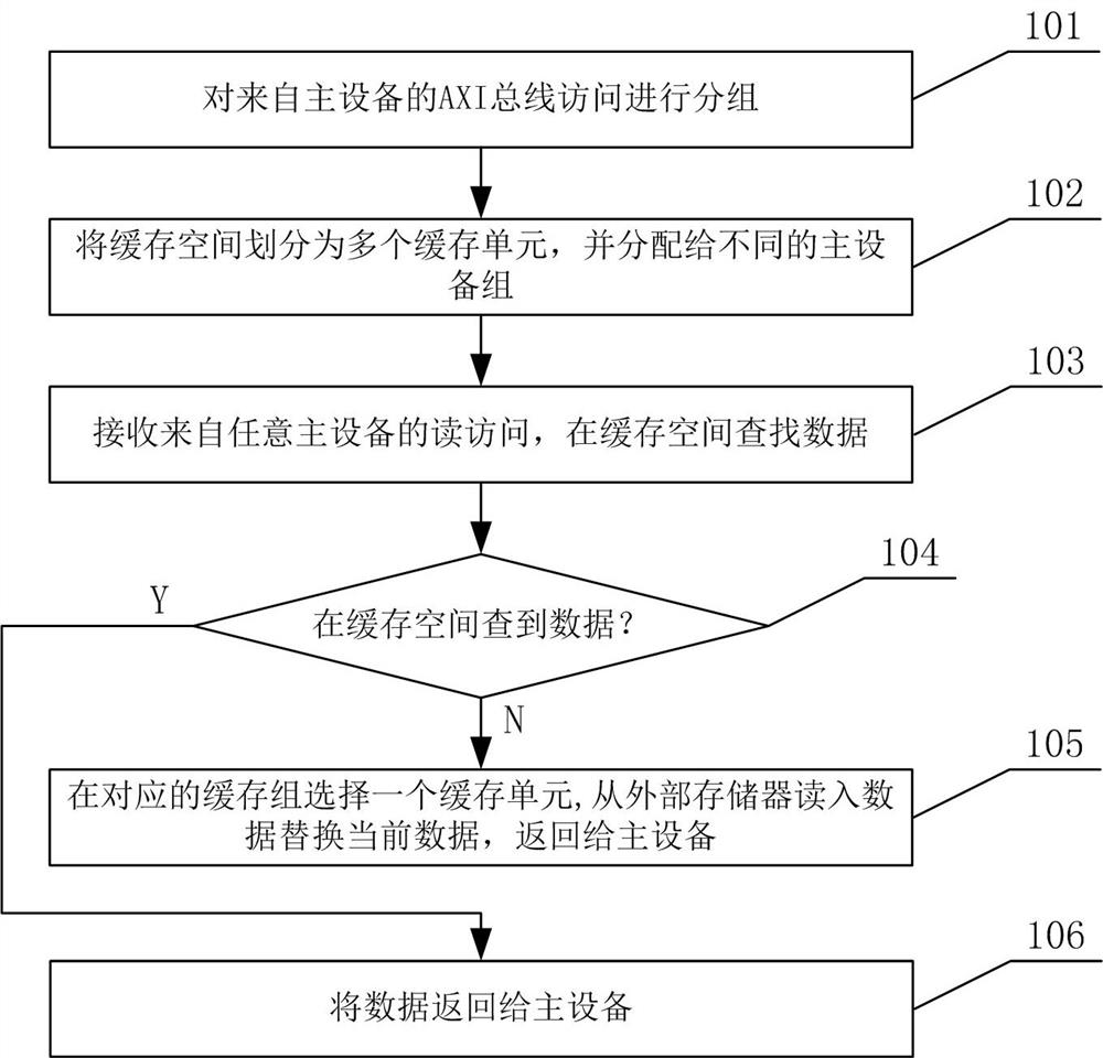
[0046] figure 1 It is a flow chart of the multi-master device cache control method according to the present invention, which will be referred to below figure 1 , the multi-master device cache control method of the present invention is described in detail.
[0047] First, in step 101, the AXI bus access from the master device is grouped.
[0048] In the embodiment of the present invention, in the scenario of multiple master devices, the AXI bus accesses from the master devices are first grouped. According to the master device ID (MID) and transmission ID (XID), combined with the group mask (Mask) and the preset matching value (Match) of each group, determine the device group (Master Group) to which an access belongs , the specific rules are as follows:
[0049] {MID, XID} & Mask == Match(M)
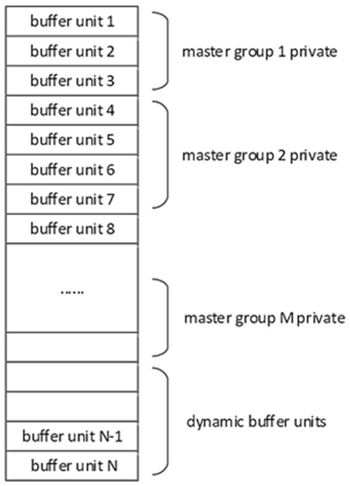
[0050] When the above conditions are met, it is considered that the device group to which the access belongs is the Mth group (group M). When multiple device groups meet the above con...
Embodiment 2
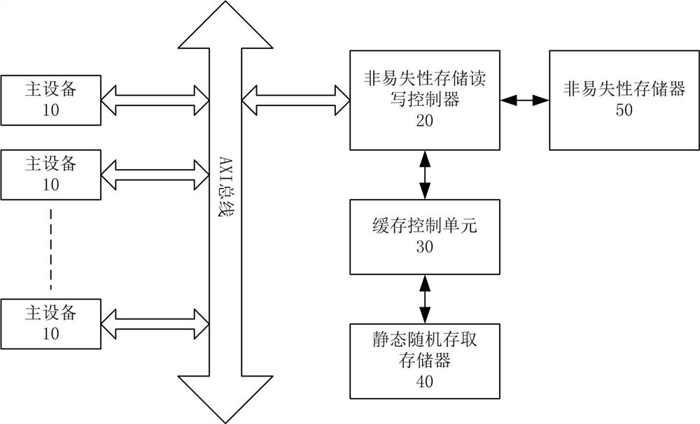
[0074] In an embodiment of the present invention, a multi-master cache control system is also provided. image 3 It is a structural diagram of a multi-master cache control system according to the present invention, such as image 3 As shown, the multi-master device cache control system of the present invention includes multiple master devices 10, non-volatile storage read-write controller 20, cache control unit 30, static random access memory 40, and non-volatile memory 50, of which,
[0075] A plurality of master devices 10, which send access requests to the non-volatile storage read-write controller 20 through the AXI bus;
[0076] The non-volatile storage read-write controller 20 groups the access requests of multiple master devices 10 .
[0077] In the embodiment of the present invention, the non-volatile storage read-write controller 20 combines the group mask (Mask) and the preset matching value of each group according to the two identifiers of the main device ID (MID)...
Embodiment 3
[0083] In one embodiment of the present invention, a control chip is also provided, including the multi-master cache control system in Embodiment 2, the multi-master cache control system, when multiple masters access the off-chip non-volatile memory , group the master devices, allocate the limited on-chip cache resources to different master device groups in static and dynamic ways, and make adaptive adjustments according to access frequency and characteristics to optimize access efficiency and reduce non-volatile memory reads Write times.
PUM
 Abstract
Description
Claims
Application Information
 - R&D
- Intellectual Property
- Life Sciences
- Materials
- Tech Scout
- Unparalleled Data Quality
- Higher Quality Content
- 60% Fewer Hallucinations
Browse by: Latest US Patents, China's latest patents, Technical Efficacy Thesaurus, Application Domain, Technology Topic, Popular Technical Reports.
© 2025 PatSnap. All rights reserved.Legal|Privacy policy|Modern Slavery Act Transparency Statement|Sitemap|About US| Contact US: help@patsnap.com