Cooling structure for enhancing heat dissipation of packaging body

A technology of cooling structure and packaging body, which is applied in the direction of electric solid-state devices, semiconductor devices, semiconductor/solid-state device components, etc., can solve the problems of no heat dissipation structure, etc., and achieve the effect of improving heat dissipation and ensuring stability

Pending Publication Date: 2022-01-11
华天科技(南京)有限公司
View PDF0 Cites 0 Cited by
  • Summary
  • Abstract
  • Description
  • Claims
  • Application Information

AI Technical Summary

Problems solved by technology

[0004] The purpose of the present invention is to overcome the above-mentioned shortcoming of the prior art, provide a kind of cooling structure that is used for strengthening the heat dissipation of package body, to solve the problem that the existing package structure in the prior art has no heat dissipation structure, the heat dissipation effect of the package structure

Method used


Image

  • Cooling structure for enhancing heat dissipation of packaging body
  • Cooling structure for enhancing heat dissipation of packaging body
  • Cooling structure for enhancing heat dissipation of packaging body

Examples


Embodiment 1

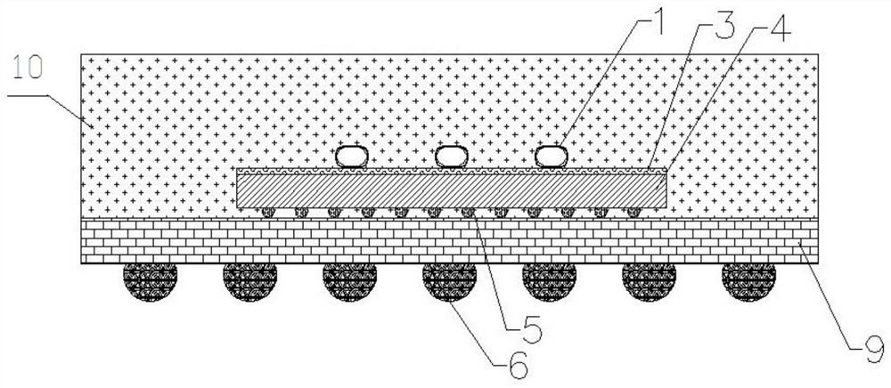
[0034] see figure 1 , image 3 and Figure 5 A metal post 5 is arranged between the lower end surface of the chip 4 and the carrier 9, and the metal post 5 can transmit electrical signals between the chip 4 and the carrier 9, so that the effective area of ​​the upper surface of the chip 4 is increased. The chip 4 is the main part of heat dissipation. When the upper surface area of ​​the chip 4 is large, the cavity pipe 1 is preferentially arranged on the upper surface of the chip 4 , and the cavity pipe 1 is attached to the upper surface of the chip 1 through the medium 3 . In order to increase the cooling area, the cavity pipe 1 is arranged in a U-shaped detour on the upper surface of the chip 4. The specific number of detours is determined according to the actual surface area of ​​the chip. The medium 3 is an adhesive with high thermal conductivity.

[0035] see image 3 , The chip 4 is provided with a cavity pipe 1, the inlet and outlet of which are respectively arranged...

Embodiment 2

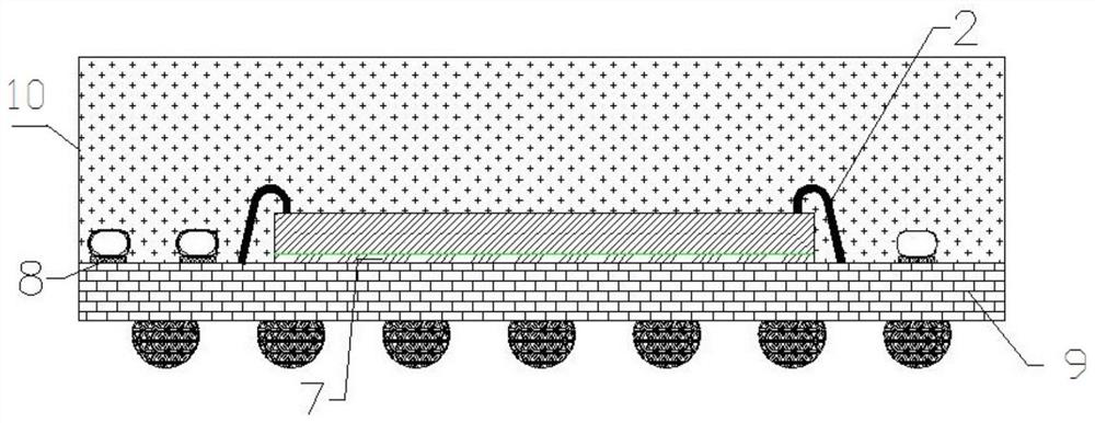
[0037] see figure 2 , Figure 4 and Figure 6 The chip 4 is pasted on the carrier board 9 through the first glue 7 , and the upper surface of the chip 4 is connected to the carrier board 9 through several bonding wires 2 for electrical signals. In this embodiment, the upper surface area of ​​the chip 4 is not large, so that the cavity pipeline 11 is not suitable for being arranged on the upper surface of the chip 4, the cavity pipeline 11 is arranged around the chip 4, and the cavity pipeline 11 is arranged in a circle around the chip 4, The cavity pipe 11 is pasted on the upper surface of the carrier plate 9 through the second glue 8, and the first glue 7 and the second glue 8 are both high thermal conductivity adhesive glue.

[0038] see Figure 6 , the chip 4 is rectangular, and the cavity pipeline 11 is arranged around the four sides of the chip 4, and the cavity pipeline 11 on each side of the chip 4 can be straight, wavy or U-shaped, and is set according to the free ...

Embodiment 3

[0041] When the chip 4 and the carrier board 9 are provided with cavity pipes 11 at the same time, the cavity pipes 11 on the chip 4 and the carrier board 9 are two separate cavity pipes 11 .

[0042] The cavity pipeline 11 on the chip 4 is connected to the chip 4 through the medium 3 , and the cavity pipeline 11 can be arranged on the chip 4 in a detour.

[0043] The cavity pipe 11 on the carrier plate 9 is connected to the carrier plate 9 through the second glue 8 , and the cavity pipe 11 is arranged around the chip 4 .

[0044] The inlet and outlet of the cavity pipeline 11 on the chip 4 are higher than the inlet and outlet of the cavity pipeline 11 on the carrier plate 9 .


PUM


Abstract

The invention discloses a cooling structure for enhancing heat dissipation of a packaging body, according to an electric connection relationship between a chip and a carrier plate, cavity pipelines are arranged at different positions, and cooling liquid is introduced into the cavity pipelines, so that the cooling liquid can cool the chip, the heat dissipation performance of the packaging body is obviously improved, and the stability of the chip during operation is ensured.

Description

technical field [0001] The invention belongs to the technical field of semiconductor packaging, and in particular relates to a cooling structure and method for enhancing the heat dissipation of a packaging body. Background technique [0002] With the rapid development of the semiconductor industry and the miniaturization of electronic products, electronic packaging products must not only provide chip protection, but also meet the ever-increasing performance, reliability, heat dissipation, electromagnetic shielding and other requirements at a certain cost. Especially in meeting the heat dissipation requirements, it poses a big challenge to the new generation of high-speed, highly integrated chips, which will directly affect the stability of the chips at high-speed operation. Therefore, in the chip industry, FC-BGA technology has been adopted. It is mainly used in display and radio frequency chip products. Based on its unique flip-chip packaging form, the back of the chip can ...

Claims


Application Information

Patent Timeline
Patent Type & Authority Applications(China)
IPC IPC(8): H01L23/473H01L23/467H01L23/31
CPCH01L23/473H01L23/467H01L23/315
Inventor 马晓建刘卫东高瑞锋杨欢张兵张红兵苏亚兰
Owner 华天科技(南京)有限公司
Why Eureka
Try Eureka