Packaging method of LED device with matte surface
A technology of LED devices and packaging methods, which is applied to semiconductor devices, electrical components, circuits, etc., can solve the problems of material and process parameter limitations, and achieve a stable matte effect
- Summary
- Abstract
- Description
- Claims
- Application Information
AI Technical Summary
Problems solved by technology
Method used
Image
Examples
Embodiment 1
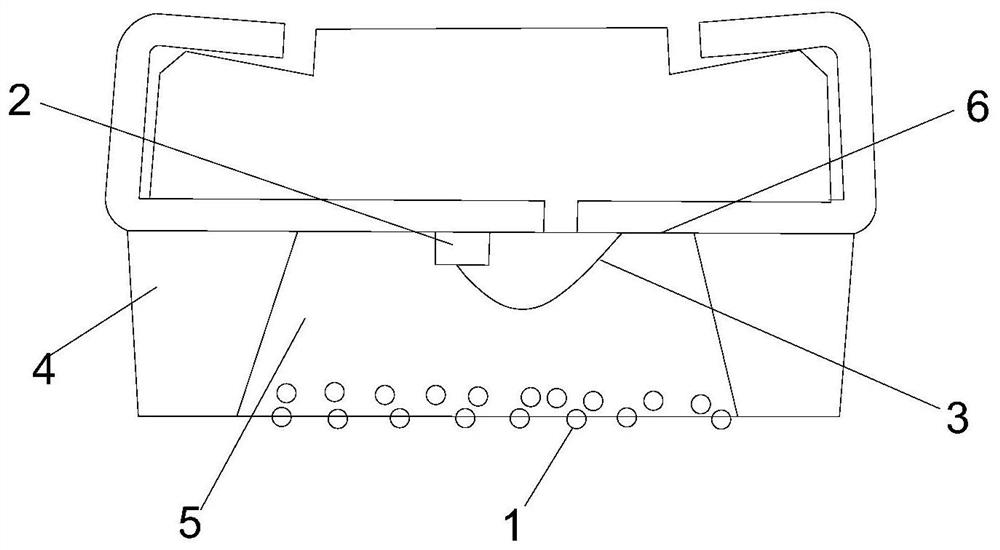
[0024] This embodiment provides a matte-surfaced LED lamp bead, which includes the following parts: LED bracket 4, LED light-emitting chip 2, wire 3 connecting LED light-emitting chip 2 and LED bracket 4, and colloid 5 covering the inside of the bowl , there are multiple silica micropowder particles 1 inside and on the surface of the colloid. In other embodiments, it can also be an LED flip-chip, so that there is no wire 3 .
[0025] In this implementation, silica powder 1 can be a solid spherical or irregular shape, deposited on the surface of the colloid in the figure, and dispersed in the interior of the colloid, its D 50 5-20μm, density 2-2.65kg / L. The colloidal surface has a surface roughness of 1-20 μm due to the action of silica micropowder.
[0026] The matte surface LED lamp bead of this embodiment, its encapsulation method comprises the following several steps:
[0027] (1) Assembling: bonding the LED light-emitting chip 2 to the support pad 6 with glue, and then ...
PUM
| Property | Measurement | Unit |
|---|---|---|
| viscosity | aaaaa | aaaaa |
| surface roughness | aaaaa | aaaaa |
Abstract
Description
Claims
Application Information
