Device and method for plasma capacitive coupling discharge copper electroplating under atmospheric pressure
A technology of plasma and capacitive coupling, which is applied in the direction of plasma, printed circuit, electrical components, etc., can solve the problems of high cost, pollution, and high process condition requirements, and achieve low requirements for equipment and environment, simple and efficient operation, and process The effect of simple process
- Summary
- Abstract
- Description
- Claims
- Application Information
AI Technical Summary
Problems solved by technology
Method used
Image

Examples
Embodiment 1
[0054] A cold plasma direct copper plating process on the inner wall of a wafer through-silicon hole, comprising the following steps:
[0055] (1) Put a silicon wafer with a through-hole structure with a diameter of 50 mm, a thickness of 0.3 mm, and a through-hole diameter of 0.15 mm into a solution of 0.1 mol / L hydrofluoric acid for 10 minutes, and the cleaned silicon wafer The circles were put into 2mol / L acetone solution and 99.7% ethanol solution for 30 minutes respectively for cleaning;
[0056] (2) Put the silicon wafer with the through-hole structure into a deionized water ultrasonic cleaning machine, ultrasonically clean it for 10 minutes, and dry the silicon wafer with nitrogen gas for 10 minutes;
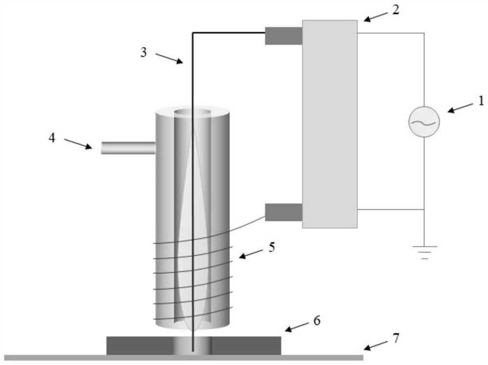
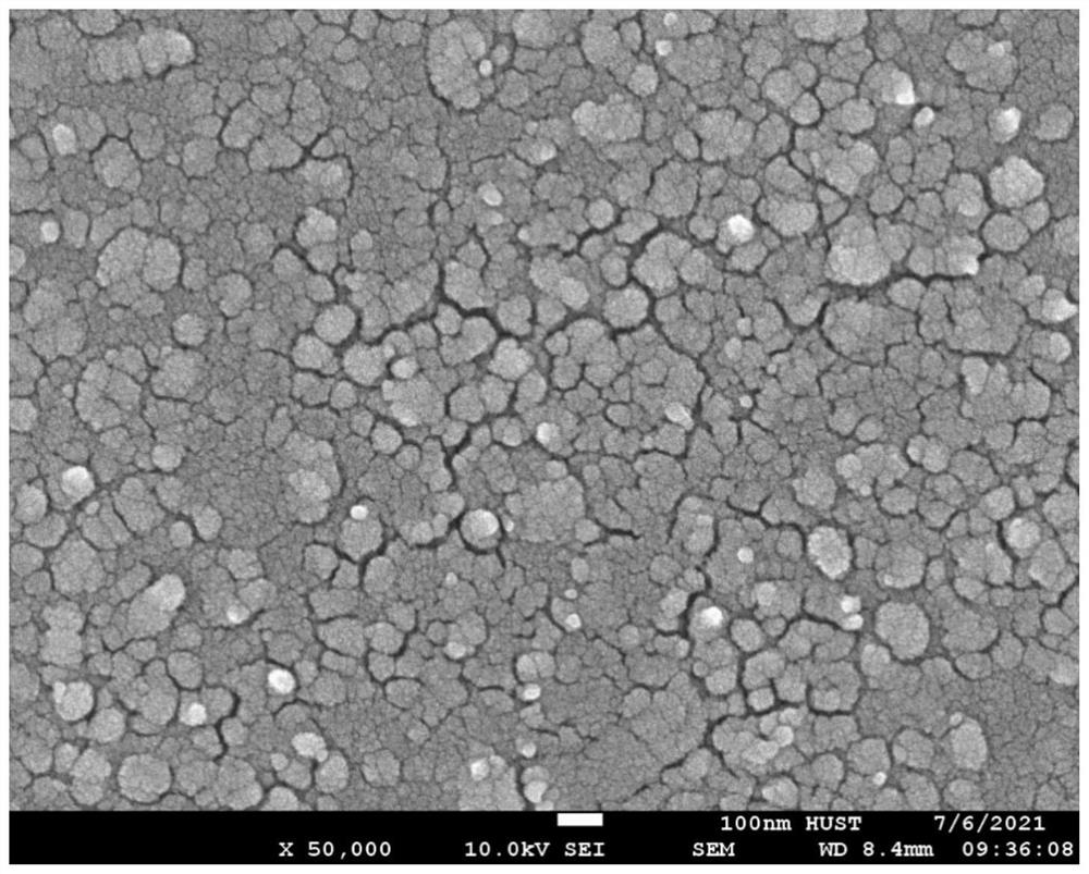
[0057] (3) Put the dried silicon wafer with the through-hole structure into such as figure 1 In the plasma capacitively coupled discharge device shown, figure 1 Among them, 1 is a radio frequency power supply, 2 is a matcher, 3 is a copper wire, 4 is a quartz tube with a...
Embodiment 2
[0060] (1) Put a silicon wafer with a through-hole structure with a diameter of 50 mm, a thickness of 0.5 mm, and a through-hole diameter of 0.3 mm into a 0.1mol / L hydrofluoric acid solution for 10 minutes, and clean the silicon wafer with a through-hole structure. The silicon wafer with the pore structure is put into 2mol / L acetone solution and 99.7% ethanol solution for 30 minutes respectively for cleaning;
[0061] (2) Put the silicon wafer with the through-hole structure into a deionized water ultrasonic cleaning machine, ultrasonically clean it for 10 minutes, and then dry the silicon wafer with the through-hole structure with nitrogen gas, and the drying time is 10 minutes ;
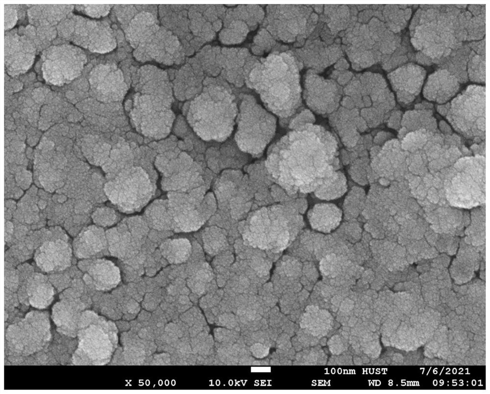
[0062] (3) Put the dried silicon wafer with through-hole structure into figure 1 In the plasma capacitively coupled discharge device shown, a silicon wafer with a through-hole structure is placed on a mechanical platform, and the coil is wound around the outside of the quartz tube. 200sccm, turn ...
PUM
| Property | Measurement | Unit |
|---|---|---|
| diameter | aaaaa | aaaaa |
Abstract
Description
Claims
Application Information
 - R&D Engineer
- R&D Manager
- IP Professional
- Industry Leading Data Capabilities
- Powerful AI technology
- Patent DNA Extraction
Browse by: Latest US Patents, China's latest patents, Technical Efficacy Thesaurus, Application Domain, Technology Topic.
© 2024 PatSnap. All rights reserved.Legal|Privacy policy|Modern Slavery Act Transparency Statement|Sitemap