Semiconductor packaging device and manufacturing method thereof.

A packaging device, semiconductor technology, applied in the direction of semiconductor/solid-state device manufacturing, semiconductor devices, semiconductor/solid-state device components, etc., can solve the problem of internal structure fracture of FOCoS packaging device, to eliminate negative effects, avoid fractures, improve The effect of product yield

Pending Publication Date: 2022-01-18
ADVANCED SEMICON ENG INC
View PDF0 Cites 0 Cited by
  • Summary
  • Abstract
  • Description
  • Claims
  • Application Information

AI Technical Summary

Problems solved by technology

The above-mentioned stress is likely to cause cracks in the internal structure of the FOCoS packaging device

Method used


Image

  • Semiconductor packaging device and manufacturing method thereof.
  • Semiconductor packaging device and manufacturing method thereof.
  • Semiconductor packaging device and manufacturing method thereof.

Examples


Embodiment Construction

[0036] The specific implementation manners of the present disclosure will be described below in conjunction with the accompanying drawings and examples. Those skilled in the art can easily understand the technical problems solved by the present disclosure and the technical effects produced through the contents recorded in this specification. It should be understood that the specific embodiments described here are only used to explain related inventions, rather than to limit the invention. In addition, for the convenience of description, only the parts related to the related invention are shown in the drawings.

[0037] It should be noted that the structures, proportions, sizes, etc. shown in the accompanying drawings of the specification are only used to match the content recorded in the specification for the understanding and reading of those skilled in the art, and are not intended to limit the implementation of the present disclosure. There are limited conditions, so it has...


PUM


Abstract

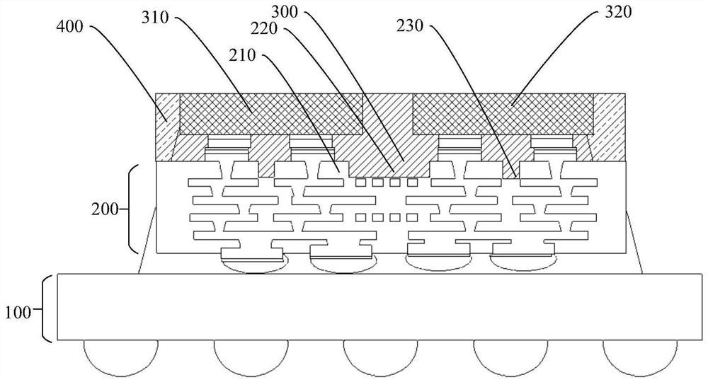
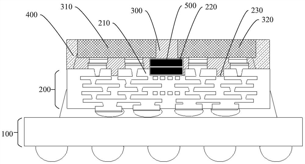
The invention relates to a semiconductor packaging device and a manufacturing method thereof. The semiconductor package device includes: a re-wiring layer having a first concave part on the surface; and a first chip and a second chip arranged on the re-wiring layer, wherein the first concave part is located below the interval between the first chip and the second chip. According to the semiconductor packaging device and the manufacturing method thereof, a larger space can be provided between the first chip and the second chip for releasing expansion stress or enhancing the structural strength, so that the negative influence of thermal stress on the structure is reduced or eliminated, breakage in the semiconductor packaging device is avoided, and the product yield is improved.

Description

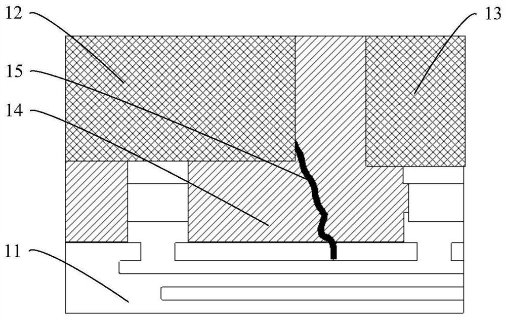
technical field [0001] The present disclosure relates to the technical field of semiconductor packaging, in particular to a semiconductor packaging device and a manufacturing method thereof. Background technique [0002] FOCoS (Fan Out Chip on Substrate) packaging technology is implemented by using a fan-out composite chip on a typical ball grid array substrate. It can provide a lower cost solution with, in practice, better electrical and thermal performance than silicon interposer structures. [0003] In the FOCoS packaging device, there is a mismatch in coefficient of thermal expansion (coefficient of thermal expansion, CTE) among various materials. During the thermal cycle process, each material will have different expansion due to the inconsistent coefficient of thermal expansion, which will cause stress inside the structure. The above-mentioned stress easily causes cracks in the internal structure of the FOCoS packaging device. [0004] Therefore, it is necessary to ...

Claims


Application Information

Patent Timeline
Patent Type & Authority Applications(China)
IPC IPC(8): H01L23/498H01L23/31H01L23/18H01L21/56
CPCH01L23/49838H01L23/49822H01L23/3114H01L23/18H01L21/563H01L2224/16225H01L2224/73204H01L2224/32225H01L2924/15311H01L2924/18161H01L2924/00
Inventor 庄劭萱张皇贤
Owner ADVANCED SEMICON ENG INC
Why Eureka
Try Eureka