
High-precision Mini-LED PCB small bonding pad windowing manufacturing method

A manufacturing method and technology of small pads, which are applied in the fields of printed circuit manufacturing, instruments, electrical components, etc., can solve problems such as shrinking of pads, strict requirements on alignment accuracy and size of solder mask window openings, increase in number and density of pads, etc. , to achieve the effect of high alignment

Active Publication Date: 2022-01-21
GUANGDONG KINGSHINE ELECTRONICS TECH CO LTD
View PDF10 Cites 1 Cited by
  • Summary
  • Abstract
  • Description
  • Claims
  • Application Information

AI Technical Summary

Problems solved by technology

[0008] The purpose of the present invention is to solve the problem of the existing Mini-LED PCB design, the increase in the number and density of pads, the shrinkage of pads, the strict requirements for ink flatness and color difference on the PCB surface, and the need for window opening for solder resist. Issues with extremely stringent bit precision and size requirements

Method used

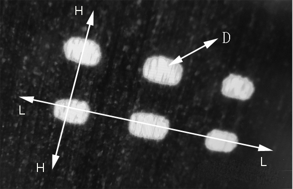
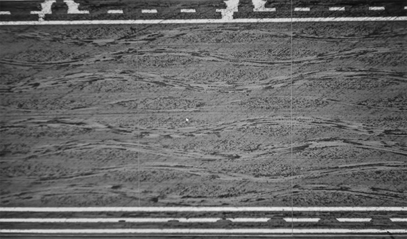
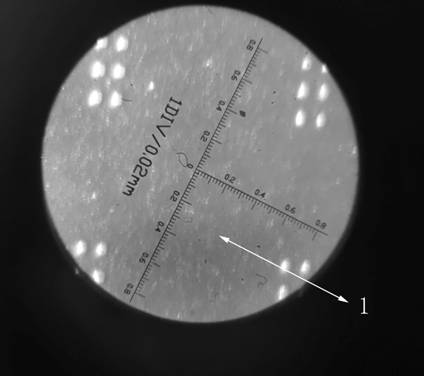

Image

  • High-precision Mini-LED PCB small bonding pad windowing manufacturing method
  • High-precision Mini-LED PCB small bonding pad windowing manufacturing method
  • High-precision Mini-LED PCB small bonding pad windowing manufacturing method

Examples


Embodiment Construction

[0047] The following will clearly and completely describe the technical solutions in the embodiments of the present invention with reference to the drawings in the embodiments of the present invention. Apparently, the described embodiments are only some of the embodiments of the present invention, but not all of them. Based on the embodiments of the present invention, all other embodiments obtained by persons of ordinary skill in the art without creative efforts fall within the protection scope of the present invention.

[0048] A method for making a small pad window opening of a high-precision Mini-LED PCB is carried out according to the following steps:

[0049] Step 1, the first pretreatment: do not open the needle and grind, open a section of volcanic ash, other parameters are normal, manually place the board, close the board and insert the rack;

[0050] Step 2, the first silk screen printing: use 43T stencil, open oil and water 30ml per kilogram, print on one side, only...


PUM


Abstract

The invention relates to a high-precision Mini-LED PCB small bonding pad windowing manufacturing method, which comprises the steps: 1, first pretreatment; 2, first silk-screen printing; 3, first exposing; 4, first developing; 5, post-baking; 6, second pretreatment; 7, second silk-screen printing; 8, second exposing; 9, second developing; 10, character jet printing; 11, baking; 12, plate grinding; 13, plasma degumming; and 14, sand blasting, and grinding out of a small bonding pad. The small bonding pad windowing has the following advantages that (1) the flatness of printing ink reduces light blocking; and (2) the ink windowing mode breaks through the minimum size of the traditional ink windowing, the alignment degree is high, and the bonding pad windowing does not deviate.

Description

technical field [0001] The invention relates to the technical field of high-precision PCB board production, and in particular to a method for manufacturing high-precision Mini-LED PCB small pad window opening. Background technique [0002] As a new generation of display technology, Mini-LED has the following technical problems in the corresponding existing Mini-LED PCB design: [0003] 1. The number and density of pads increase geometrically; [0004] 2. Wafer size (such as 3*6mil) and pads are smaller than ordinary wafer size (such as 4*8mil) and pads (that is to say, the size of the wafer is reduced, and the size of the corresponding pad is also reduced); [0005] 3. Due to the optical characteristics, Mini-LED has strict requirements on the ink flatness and color difference on the PCB surface; [0006] 4. Mini-LED has extremely strict requirements on the alignment accuracy and size of the solder resist window opening. [0007] In order to overcome the above-mentioned p...

Claims


Application Information

Patent Timeline
IPC IPC(8): H05K3/40G09F9/33H01L33/62
CPCH05K3/4007G09F9/33H01L33/62
Inventor 王欣陈子濬颜怡锋
Owner GUANGDONG KINGSHINE ELECTRONICS TECH CO LTD
Learn More