
Manufacturing method of PCB equilateral triangle

An equilateral triangle and manufacturing method technology, which is applied in chemical/electrolytic methods to remove conductive materials, printed circuit manufacturing, computer design circuits, etc. Avoid abnormal appearance and improve accuracy

Pending Publication Date: 2022-02-08
JIANGSU PROVISION ELECTRONICS CO LTD
View PDF8 Cites 0 Cited by
  • Summary
  • Abstract
  • Description
  • Claims
  • Application Information

AI Technical Summary

Problems solved by technology

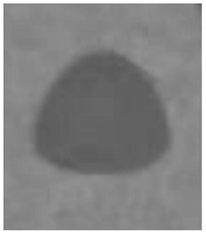
[0002] The alignment standards of products related to the electronics industry are becoming smaller and smaller, and the uniformity of etching control is used more frequently, which poses more and more challenges to the design and process. In the existing technology, the standard isosceles is directly designed. The triangle is etched, but the etching control image is affected by the gutter effect—that is, the amount of etching in the dense area and the open area is different. The actual etched triangle presents a figure with a large middle and missing sharp corners, such as figure 1 As shown, it is impossible to accurately produce the inscribed circle and circumscribed circle of the size required by the customer

Method used


Image

  • Manufacturing method of PCB equilateral triangle
  • Manufacturing method of PCB equilateral triangle
  • Manufacturing method of PCB equilateral triangle

Examples


Embodiment

[0031] Example: such as Figure 1-5 Shown, a kind of manufacturing method of PCB equilateral triangle comprises the following steps:

[0032] Step 1: Cutting and baking: Cut the PCB into a certain size and bake it in an oven; the purpose of cutting is to facilitate subsequent equipment processing; the baking conditions are: temperature 122-148°C, The baking time is 2-4h; the substrate is baked to eliminate the stress of the substrate to prevent the substrate from warping, improve the dimensional stability of the substrate, and reduce the expansion and contraction of the substrate;

[0033] Step 2: Drilling: Use a drilling machine to drill multiple positioning holes on the PCB;

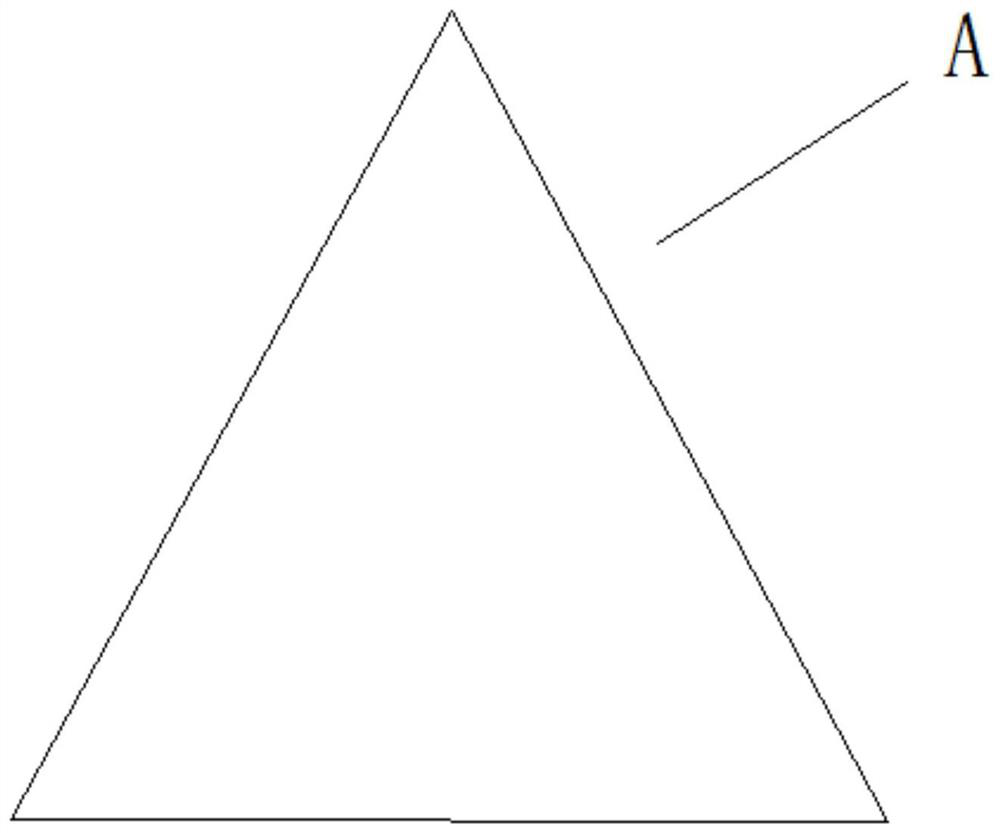
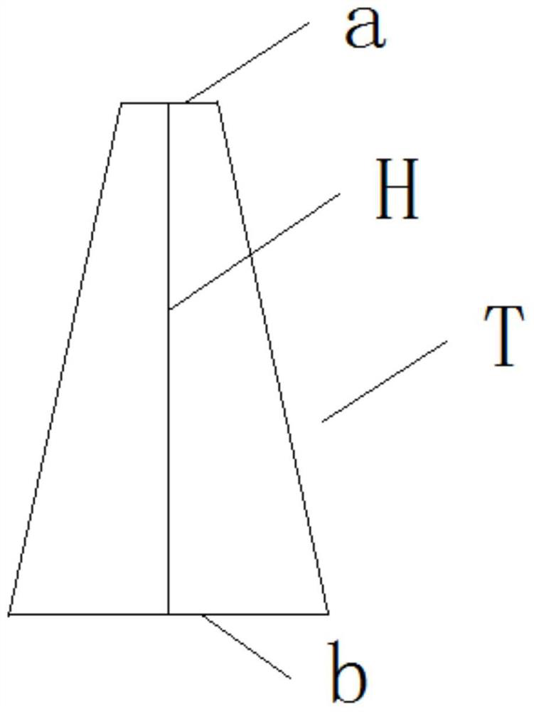
[0034] Step 3: graphic design: according to the design standard, use software to draw an equilateral triangle A (such as figure 2 shown) and isosceles trapezoidal T (such as image 3 shown), and form a new design graphic B (such as Figure 4 shown), the new design figure is composed of the equilat...


PUM


Abstract

The invention relates to a manufacturing method of a PCB equilateral triangle, and the method comprises the following steps: cutting and baking: cutting a PCB into a certain size, and putting the PCB into a baking oven for baking; drilling: drilling a plurality of positioning holes in the PCB by using a drilling machine; graphic design: drawing an equilateral triangle and an isosceles trapezoid by using software according to a design standard and forming a new design graph, and circuit exposure: capturing a mechanical positioning hole for positioning according to design data, transferring the design graph to the PCB by using photochemical reaction, and dissolving a design image data graph by reacting unexposed components in a dry film with weak base; and pattern etching: enabling the exposed copper surface to be in contact with an etching solution, and forming the required equilateral triangle hollow forming effect through the effect of dissolving and corroding copper. A finished product pattern etched by utilizing the pattern designed by the invention is closer to an equilateral triangle, and the sharp corner has an appearance, so that the requirement of the design appearance is met.

Description

technical field [0001] The invention relates to a PCB board, in particular to a method for manufacturing a PCB equilateral triangle. Background technique [0002] The alignment standards of products related to the electronics industry are becoming smaller and smaller, and the uniformity of etching control is used more frequently, which poses more and more challenges to the design and process. In the existing technology, the standard isosceles is directly designed. The triangle is etched, but the etching control image is affected by the gutter effect—that is, the amount of etching in the dense area and the open area is different. The actual etched triangle presents a figure with a large middle and missing sharp corners, such as figure 1 As shown, it is impossible to accurately produce inscribed circles and circumscribed circles of the size required by customers. Contents of the invention [0003] In order to overcome the above-mentioned defects, the present invention provi...

Claims


Application Information

Patent Timeline
Patent Type & Authority Applications(China)
IPC IPC(8): H05K3/00H05K3/06
CPCH05K3/0005H05K3/06H05K2201/09209
Inventor 马洪伟郭周杨
Owner JIANGSU PROVISION ELECTRONICS CO LTD
Learn More