Chip packaging structure

A technology of chip packaging structure and chip body, which is applied in the direction of electrical components, electric solid devices, circuits, etc., can solve the problems of unstable packaging structure, chip loosening and shifting, and affecting the normal use of circuit boards, so as to improve the protection stability and The effect of sealing reliability and preventing loosening and displacement

Pending Publication Date: 2022-02-11
武汉烽唐科技有限公司
View PDF0 Cites 0 Cited by
  • Summary
  • Abstract
  • Description
  • Claims
  • Application Information

AI Technical Summary

Problems solved by technology

However, in the existing surface mount technology, due to the continuous reduction of chip size, it brings greater challenges to the implementation of the manufacturin

Method used


Image

  • Chip packaging structure
  • Chip packaging structure
  • Chip packaging structure

Examples


Embodiment Construction

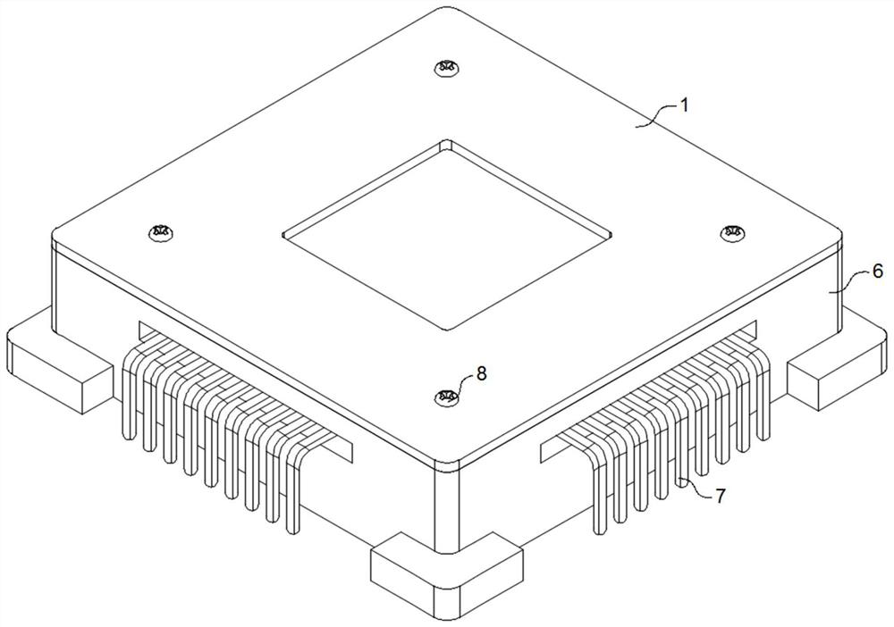
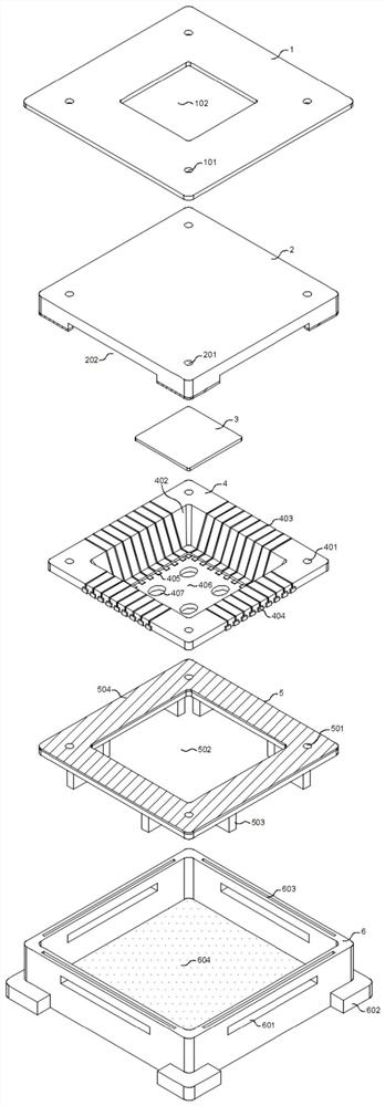
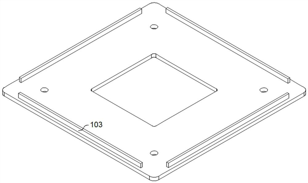
[0022] The following will clearly and completely describe the technical solutions in the embodiments of the present invention with reference to the accompanying drawings in the embodiments of the present invention. Obviously, the described embodiments are only part of the embodiments of the present invention, not all of them. In the case of no conflict, the embodiments in the present application and the features in the embodiments can be combined with each other. Based on the embodiments of the present invention, all other embodiments obtained by persons of ordinary skill in the art without creative efforts fall within the protection scope of the present invention.

[0023] It should be noted that if there is a directional indication (such as up, down, left, right, front, back...) in the embodiment of the present invention, the directional indication is only used to explain the position in a certain posture (as shown in the accompanying drawing). If the specific posture change...


PUM


Abstract

A chip packaging structure disclosed by the present invention comprises a cover plate, a cover plate, a chip body, a substrate, a supporting plate and a base, the middle part of the substrate is provided with an inner concave cavity, the chip body is fixed in the inner concave cavity, the cover plate is pressed on the top surface of the substrate, the supporting plate is connected to the bottom surface of the substrate, the supporting plate is installed in the base, and the cover plate is attached to the upper surface of the cover plate and matched with the base in a clamped mode. According to the invention, the substrate with the concave cavity structure is adopted to fix and paste the chip body, so that limiting installation is facilitated in the packaging process, and the cover plate, the substrate and the supporting plate are sequentially nested and inserted from top to bottom to form a stable interlayer whole, so that the chip body is effectively prevented from loosening and shifting; after the interlayer is integrally fixed in the cover plate and the base, compact and firm packaging is carried out, a simple and light integral structure is formed, and the protection stability and the sealing reliability of the integral structure of the device can be improved.

Description

technical field [0001] The invention relates to the technical field of chip packaging, in particular to a chip packaging structure. Background technique [0002] In the industrial chain of the overall production of integrated circuits, chip packaging has always been an important link. The so-called package refers to the shell used to install the semiconductor integrated circuit chip. It not only plays the role of placing, fixing, sealing, protecting the chip and enhancing thermal conductivity, but also bridges the internal world of the chip and the external circuit, that is, the contacts on the chip use wires. It is connected to the pins of the package shell, and then the pins establish a connection relationship with other devices through the wires on the printed board. [0003] Chip packaging plays an important role in CPUs and other LSI integrated circuits, and the emergence of a new generation of CPUs is often accompanied by the use of new packaging forms. Chip packagin...

Claims


Application Information

Patent Timeline
IPC IPC(8): H01L23/047H01L23/043H01L23/04
CPCH01L23/047H01L23/043H01L23/04
Inventor 李可
Owner 武汉烽唐科技有限公司
Why Eureka
Try Eureka