
Use method of electronic chip fixing device with overload protection structure

A technology for electronic chips and fixing devices, which is applied in the field of electronic chip fixing devices with overload protection structures, can solve problems such as easy blockage of filter screens and ineffective heat dissipation operations, and achieve the effect of protecting normal use

Active Publication Date: 2022-02-15
NANTONG MINICHIP MICRO ELECTRONICS
View PDF8 Cites 0 Cited by
  • Summary
  • Abstract
  • Description
  • Claims
  • Application Information

AI Technical Summary

Problems solved by technology

The structure design of the invention is simple and reasonable, easy to operate, easy to disassemble and fix, good heat dissipation effect, safe and stable, wide application range, and conducive to promotion and popularization". In turn, the filter screen of the device is prone to blockage during subsequent use, making the heat dissipation operation of the device unable to be carried out effectively

Method used


Image

  • Use method of electronic chip fixing device with overload protection structure
  • Use method of electronic chip fixing device with overload protection structure
  • Use method of electronic chip fixing device with overload protection structure

Examples


Embodiment 1

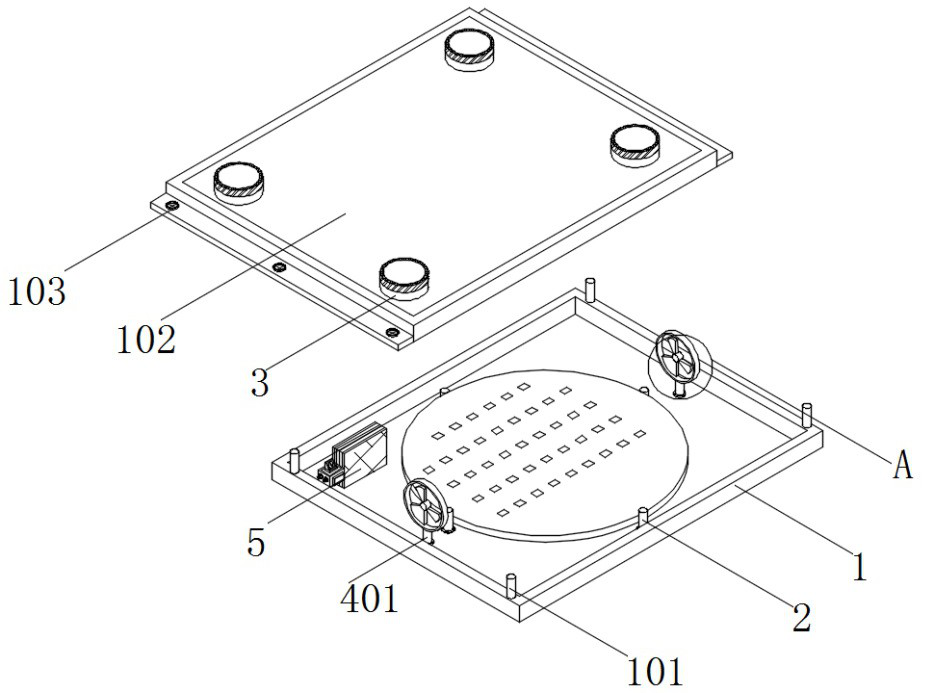
[0045] see figure 1 with Image 6 , an embodiment provided by the present invention: a method for using an electronic chip fixing device with an overload protection structure, comprising a protective housing 1 and an overload protection unit 5, the inner bottom wall of the protective housing 1 is equipped with an overload protection unit 5, And the overload protection unit 5 is located at the rear of one of the turntables 4, the overload protection unit 5 includes a diode plate 501, an ammeter 502, a rectifier 503 and a commutator 504, and a rectifier 503 is installed on the surface of the diode plate 501, and the rectifier 503 An ammeter 502 is installed on the top, and a commutator 504 is installed on the front of the rectifier 503;

[0046] The output terminal of the ammeter 502 is electrically connected to the input terminal of the rectifier 503 , the output terminal of the rectifier 503 is connected to the input terminal of the commutator 504 , and the output terminal of...

Embodiment 2

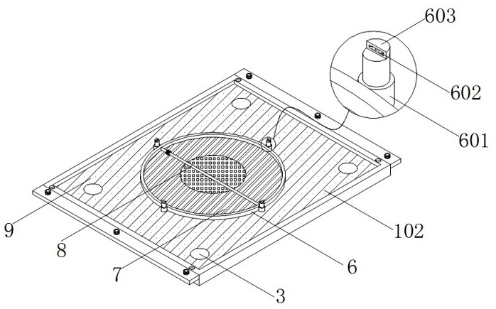
[0050] see figure 1 , Figure 7 with Figure 8 , an embodiment provided by the present invention: a method of using an electronic chip fixing device with an overload protection structure, including a rust removal slide bar 8 and a dust collection frame plate 7, and the inner wall of the limit hoop 6 is installed with a symmetrical arrangement The iron plate 805 of two groups of iron plates 805 is installed with derusting slide bar 8 on the surface close to each other, and the surface of derusting slide bar 8 is slidingly sleeved with slide block 802, and the surface of slide block 802 is surrounded with sandpaper layer 801, and The length of sandpaper layer 801 is less than the length of slide block 802, and the surface of slide block 802 is equipped with laser rangefinder 804, and laser rangefinder 804 is positioned at the side of sandpaper layer 801, and the surface of both sides of slide block 802 is all installed with etc. The electromagnetic column 803 arranged at a dis...

Embodiment 3

[0056] see figure 2 , an embodiment provided by the present invention: a method of using an electronic chip fixing device with an overload protection structure, including a limit hoop 6, a fitting 101 is installed on the top of the frame of the protective shell 1, and the protective shell 1 The top is connected with a top cover 102 through a fitting 101, and the inner top wall of the top cover 102 is equipped with a limit hoop 6, and the surface of the limit hoop 6 is equidistantly equipped with an electric telescopic rod 601, and the bottom of the electric telescopic rod 601 A semicircular clamping block 603 is installed, and the rectangular surface of the clamping block 603 is fitted with an indented pressure sensor 602 .

[0057] Both side outer walls of the top cover 102 are provided with connecting plates 103 , and connecting bolts are installed inside the connecting plates 103 .

[0058] Specifically, the fitting connection between the protective shell 1 and the top co...


PUM


Abstract

The invention discloses a use method of an electronic chip fixing device with an overload protection structure, and the device comprises a protection shell, the inner bottom wall of the protection housing is provided with rubber columns which are arranged at equal intervals, the inner bottom wall of the protection housing is provided with symmetrically arranged turntables, and the inner bottom wall of the protection housing is provided with an overload protection unit. The overload protection unit comprises a diode plate, an ampere meter, a rectifier and a commutator, the rectifier is installed on the surface of one side of the diode plate, the ampere meter is installed on the top of the rectifier, and the commutator is installed on the front face of the rectifier. By arranging the overload protection unit, when the ampere meter detects that the instantaneous current is relatively large, the rectifier can be started to realize alternating current-direct current change, then the direction is changed through the commutator, then the instantaneous current is connected with the diode plate, and on the premise that the current direction is changed, the access current value of the electronic chip is reduced, and corresponding overload protection is realized.

Description

technical field [0001] The invention relates to the technical field of chip fixing, in particular to a method for using an electronic chip fixing device with an overload protection structure. Background technique [0002] With the development of science and technology, more and more electronic products are flooding our lives, bringing great convenience to our lives. Among them, the realization of the functions of electronic products mainly depends on the internal new electronic products, the surface of electronic chips Integrated circuits are arranged to assist electronic products to achieve corresponding functional instructions. Therefore, electronic chips are of great significance to ensure the normal use of electronic products. When electronic chips are installed inside electronic products, a fixing device is needed to ensure the stability of electronic chips. Install. [0003] The defective that existing chip fixing device exists is: [0004] 1. The comparative documen...

Claims


Application Information

Patent Timeline
Patent Type & Authority Applications(China)
IPC IPC(8): H01L21/687H02H9/02B24B27/033B24B49/12B01D46/10B01D46/00H05K7/20
CPCH01L21/68785H02H9/02B24B27/033B24B49/12B01D46/10B01D46/0086H05K7/20181
Inventor 周明
Owner NANTONG MINICHIP MICRO ELECTRONICS
Learn More