A method of using an electronic chip fixing device with an overload protection structure
An electronic chip, overload protection technology, applied in emergency protection circuit devices, emergency protection circuit devices for limiting overcurrent/overvoltage, circuit devices, etc. problem, to protect the effect of normal use
- Summary
- Abstract
- Description
- Claims
- Application Information
AI Technical Summary
Problems solved by technology
Method used
Image
Examples
Embodiment 1
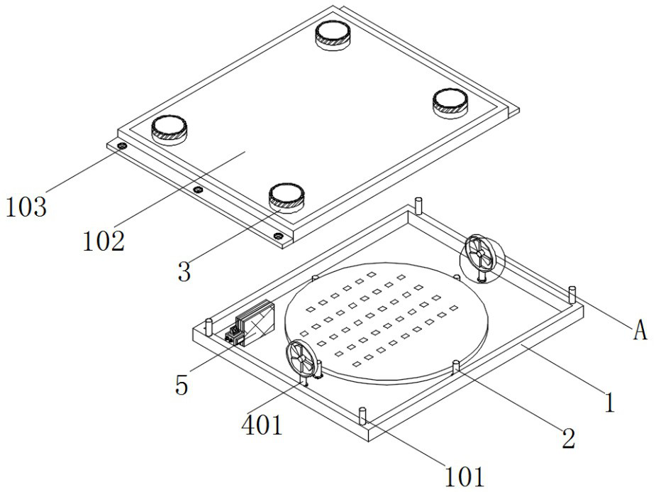
[0045] See Figure 1 and Figure 6 , one embodiment of the present invention provided: a method of use of an electronic chip fixture with an overload protection structure, comprising a protective housing 1 and an overload protection unit 5, the inner bottom wall of the protective housing 1 is installed with an overload protection unit 5, and the overload protection unit 5 is located behind one set of turntables 4, the overload protection unit 5 includes a diode plate 501, a ammeter 502, a rectifier 503 and a commutator 504, a rectifier 503 is mounted on one side of the diode plate 501, Rectifier 503 is installed on the top of the ammeter 502, rectifier 503 is mounted on the front of the commutator 504;
[0046] The output terminal of the ammeter 502 is electrically connected to the input terminal of the rectifier 503, the output terminal of the rectifier 503 is connected to the input terminal of the commutator 504, the output terminal of the commutator 504 is electrically connecte...
Embodiment 2
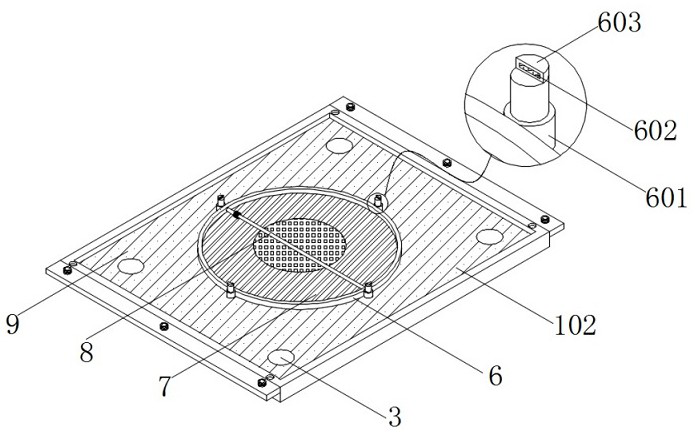
[0050] See Figure 1 、 Figure 7 and Figure 8 , one embodiment of the present invention provided: a method of use of an electronic chip fixture with an overload protection structure, comprising a rust removal slider 8 and a dust collection frame plate 7, the inner wall of the limit hoop 6 is installed with a symmetrically arranged iron plate 805, two sets of iron plates 805 are installed on the surface adjacent to each other with a rust removal slider 8, the surface sliding socket of the rust removal slider 8 is connected with a slider 802, the surface of the slider 802 is surrounded by an abrasive layer 801, and the length of the sandpaper layer 801 is less than the length of the slider 802, The surface of the slider 802 is equipped with a laser rangefinder 804, and the laser rangefinder 804 is located on one side of the sandpaper layer 801, both sides of the slider 802 are equipped with an equidistant arrangement of the electromagnetic column 803, and the electromagnetic column ...
Embodiment 3
[0056] See Figure 2 , one embodiment of the present invention provided: a method of use of an electronic chip fixture with an overload protection structure, comprising a limiting hoop 6, the top of the frame of the protective housing 1 is mounted with a chimeric member 101, the top of the protective housing 1 is connected to the top cover 102 by chimering 101, the inner top wall of the top cover 102 is mounted with a finite clamp 6, the surface of the limiting hoop 6 is isometrically mounted with an electric telescopic rod 601, the bottom of the electric telescopic rod 601 is mounted with a semicircular clamp 603, The rectangular surface of the clamp block 603 is embedded with a pressure sensor 602 embedded in the insert.
[0057] The outer walls of both sides of the top cover 102 are equipped with a connection plate 103, and the connection plate 103 is installed with connection bolts throughout the interior.
[0058] Specifically, the chimeric connection between the protective h...
PUM
 Abstract
Description
Claims
Application Information


