
Patsnap Eureka
For R&D, Patsnap Eureka makes reading and utilizing patents & technical documents easy.
Patsnap Eureka AIR
Designed for self-driven R&D workflows. Generate viable solutions, solve complex R&D challenges, empower your innovation with AI.

Patsnap Eureka Materials
Designed for material experts only. Revolutionize your material R&D, from search, analyze, to developing new materials.

TechResearch
Generate reliable direction feasibility study reports for your R&D in just a few steps.

TechSeek
Discover and master advanced knowledge NOW. Basics, ideas, possibilities, all at once.

TechMind
As an expert in R&D Theories, TechMind can generates customized viable solutions instantly.

TechRisk
Analyze your overall solution with one click, know your potential R&D risks in advance.

TechMonitor
Get weekly tech updates, stay abreast of the latest tech innovations and key insights.
Semiconductor memory devices
A semiconductor and memory technology, applied in the field of three-dimensional semiconductor memory devices, can solve problems such as limited integration
- Summary
- Abstract
- Description
- Claims
- Application Information
AI Technical Summary
Problems solved by technology
Method used
Image

Examples
Embodiment Construction
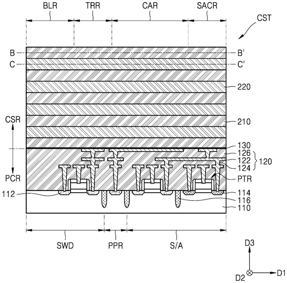
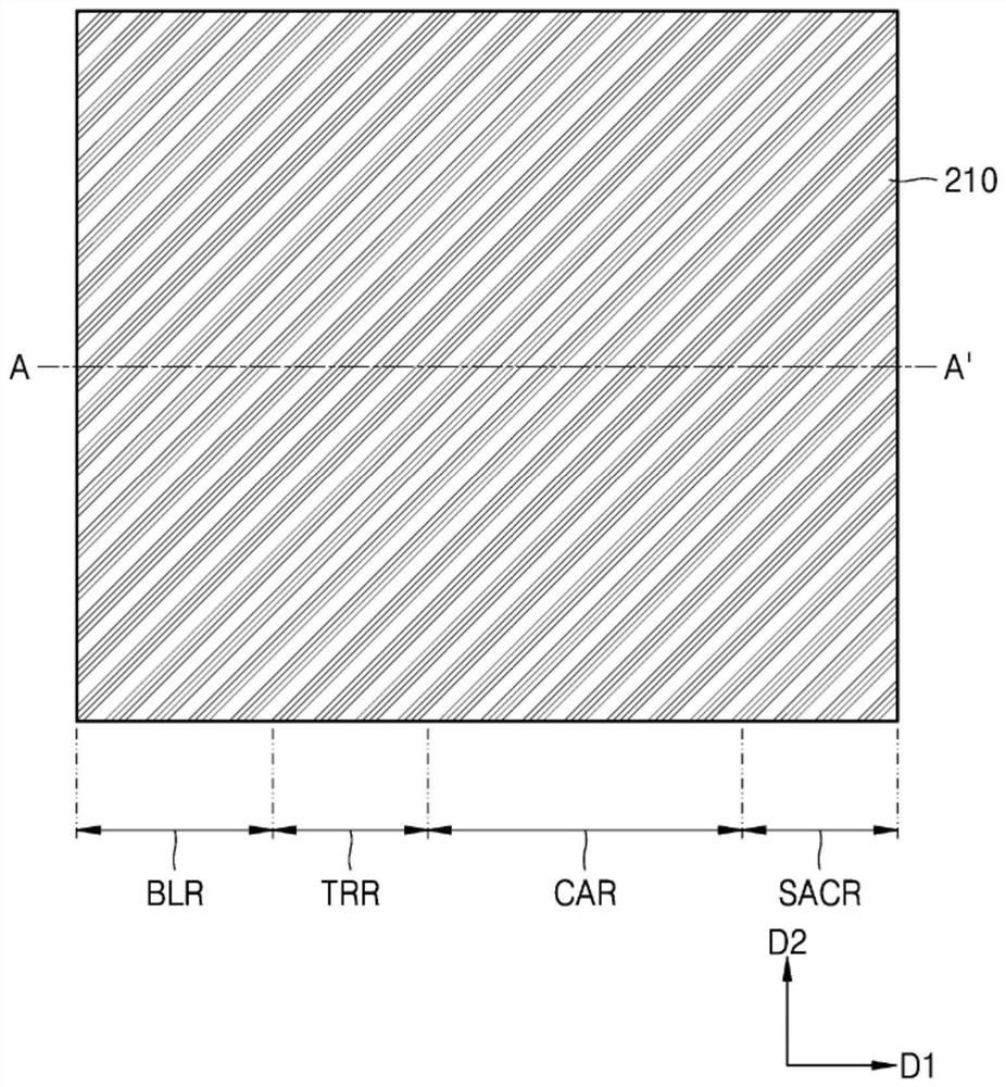
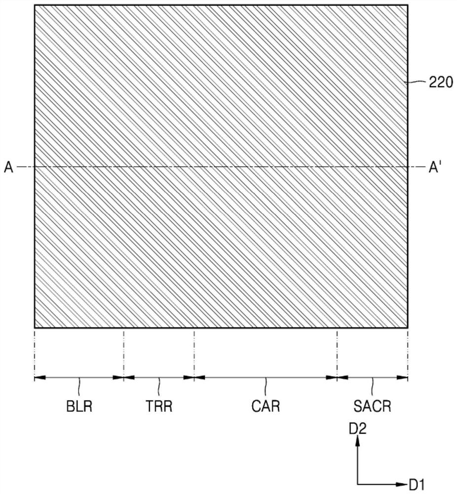
[0018] Figure 1A to Figure 20C is a diagram illustrating a method of manufacturing a semiconductor memory device according to an embodiment. in detail, Figure 1A , Figure 2A , Figure 3A , Figure 4A , Figure 5A , Figure 6A , Figure 7A , Figure 8A , Figure 9A , Figure 10A , Figure 11A , Figure 12A , Figure 13A , Figure 14A , Figure 15A , Figure 16A , Figure 17A , Figure 18A , Figure 19A and Figure 20A are shown respectively along the Figure 1B and Figure 1C , Figure 2B and Figure 2C , Figure 3B and Figure 3C , Figure 4B and Figure 4C , Figure 5B and Figure 5C , Figure 6B and Figure 6C , Figure 7B and Figure 7C , Figure 8B and Figure 8C , Figure 9B and Figure 9C , Figure 10B and Figure 10C , Figure 11B and Figure 11C , Figure 12B and Figure 12C , Figure 13B and Figure 13C , Figure 14B and Figure 14C , Figure 15B and Figure 15C , Figure 16B and Figure 16C , Figure 17B and Figu...
PUM
| Property | Measurement | Unit |
|---|---|---|
| energy | aaaaa | aaaaa |
Abstract
Description
Claims
Application Information
 - R&D Engineer
- R&D Manager
- IP Professional
- Industry Leading Data Capabilities
- Powerful AI technology
- Patent DNA Extraction
Browse by: Latest US Patents, China's latest patents, Technical Efficacy Thesaurus, Application Domain, Technology Topic, Popular Technical Reports.
© 2024 PatSnap. All rights reserved.Legal|Privacy policy|Modern Slavery Act Transparency Statement|Sitemap|About US| Contact US: help@patsnap.com