Optical material filling method and device

A technology of optical materials and filling methods, applied in electrical components, electric solid devices, circuits, etc., can solve the problem of difficult filling of optical materials

Pending Publication Date: 2022-02-25
BEIJING IVISUAL 3D TECH CO LTD
View PDF0 Cites 0 Cited by
  • Summary
  • Abstract
  • Description
  • Claims
  • Application Information

AI Technical Summary

Problems solved by technology

[0004] The filling of optical materials is more difficult

Method used


Image

  • Optical material filling method and device
  • Optical material filling method and device
  • Optical material filling method and device

Examples


Embodiment Construction

[0026] In order to understand the characteristics and technical content of the embodiments of the present disclosure in more detail, the implementation of the embodiments of the present disclosure will be described in detail below in conjunction with the accompanying drawings. The attached drawings are only for reference and description, and are not intended to limit the embodiments of the present disclosure. In the following technical description, for purposes of explanation, numerous details are set forth in order to provide a thorough understanding of the disclosed embodiments. However, at least one embodiment can be practiced without these details. In other instances, well-known structures and devices may be shown simplified in order to simplify the drawings.

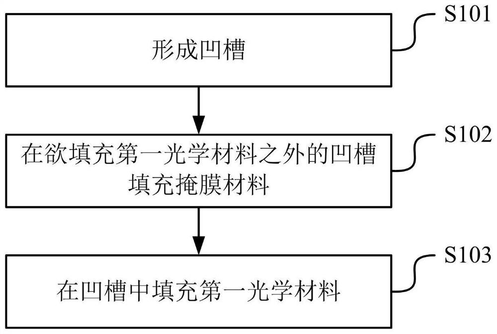
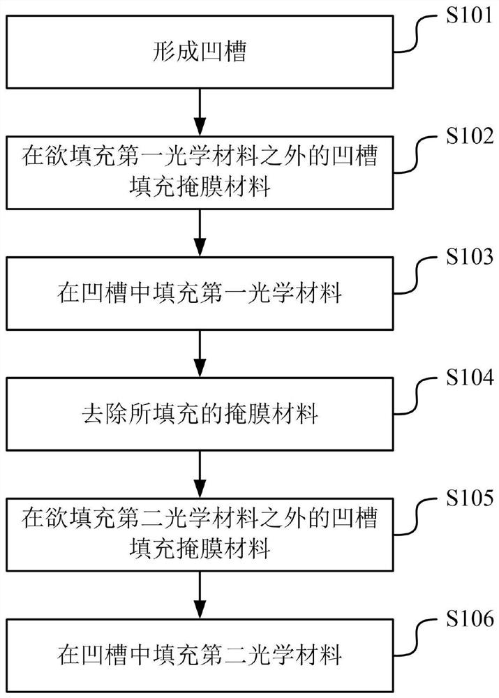
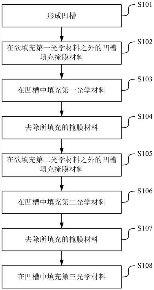
[0027] figure 1 A schematic flow chart showing the implementation of the optical material filling method provided by the embodiment of the present disclosure is shown.

[0028] As shown in the figure, an embodimen...


PUM


Abstract

The invention discloses an optical material filling method and device. The method comprises the steps of forming grooves; filling grooves except grooves to be filled with first optical materials with mask materials; and filling the grooves with the first optical materials . According to the scheme provided by the invention, the filling difficulty of the optical material is reduced to a certain extent.

Description

technical field [0001] The present application relates to the field of display technology, for example, to an optical material filling method and device. Background technique [0002] Compared with the pixel size of about 0.2mm in traditional liquid crystal display, the advantage of microLED display is that the size of a single light-emitting unit is generally less than 50um, and can even be as small as a few microns. [0003] In the process of implementing the embodiments of the present disclosure, it is found that at least the following problems exist in related technologies: [0004] The filling of optical materials is more difficult. Contents of the invention [0005] In order to provide a basic understanding of some aspects of the disclosed embodiments, a brief summary is presented below. This summary is not intended to be an extensive overview or to identify key / critical elements or to delineate the scope of these embodiments, but rather serves as a prelude to the ...

Claims


Application Information

Patent Timeline
Patent Type & Authority Applications(China)
IPC IPC(8): H01L33/00H01L25/16H01L25/00
CPCH01L33/005H01L33/0095H01L25/167H01L25/50H01L25/16H01L25/00H01L33/00
Inventor 不公告发明人
Owner BEIJING IVISUAL 3D TECH CO LTD
Why Eureka
Try Eureka