Supercharge Your Innovation With Domain-Expert AI Agents!

Circuit board structure and manufacturing method thereof

A manufacturing method and circuit board technology, applied in the structural connection of printed circuits, printed circuit manufacturing, multi-layer circuit manufacturing, etc., can solve the problems of unable to release the stress of the circuit board, reduce the assembly yield of the circuit board, etc., and reduce the production cost , The effect of improving the reliability of the structure

Pending Publication Date: 2022-03-01
UNIMICRON TECH CORP
View PDF0 Cites 0 Cited by
  • Summary
  • Abstract
  • Description
  • Claims
  • Application Information

AI Technical Summary

Problems solved by technology

However, in the process of solder reflow at high temperature, the circuit board with a large area size cannot be released due to the stress, so it is prone to large warpage, thereby reducing the assembly yield between the two circuit boards

Method used


Image

  • Circuit board structure and manufacturing method thereof
  • Circuit board structure and manufacturing method thereof
  • Circuit board structure and manufacturing method thereof

Examples


Embodiment Construction

[0059] Reference will now be made in detail to the exemplary embodiments of the present invention, examples of which are illustrated in the accompanying drawings. Wherever possible, the same reference numbers will be used in the drawings and description to refer to the same or like parts.

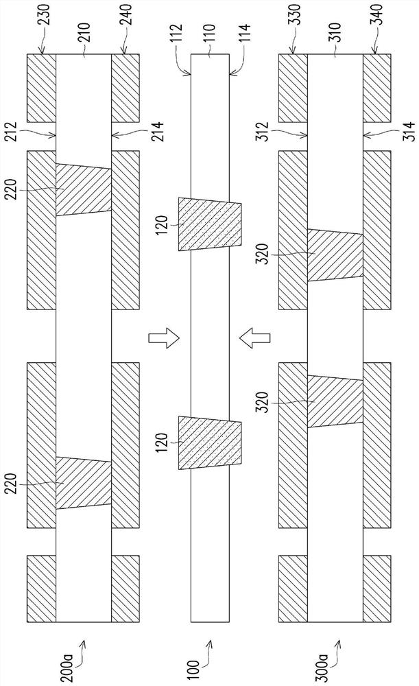
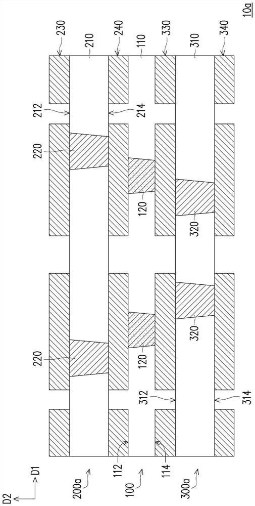
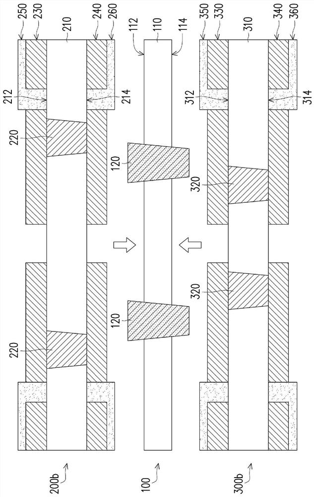
[0060] Figure 1A to Figure 1B is a schematic cross-sectional view of a manufacturing method of a circuit board structure according to an embodiment of the present invention. Regarding the manufacturing method of the circuit board structure of this embodiment, at first, please refer to Figure 1A , providing a first sub-circuit board 100 . In detail, the first sub-circuit board 100 includes a base material 110 and at least one first conductive via (two first conductive vias 120 are schematically shown). The substrate 110 has an upper surface 112 and a lower surface 114 opposite to each other. The first conductive via 120 penetrates through the substrate 110 and protrudes from the upper sur...


PUM


Abstract

The invention provides a circuit board structure and a manufacturing method thereof. The circuit board structure comprises a first sub-circuit board, a second sub-circuit board and a third sub-circuit board. The first sub-circuit board is provided with an upper surface and a lower surface which are opposite to each other, and comprises at least one first conductive through hole. The second sub-circuit board is arranged on the upper surface of the first sub-circuit board and comprises at least one second conductive through hole. The third sub-circuit board is arranged on the lower surface of the first sub-circuit board and comprises at least one third conductive through hole. At least two of the first conductive through holes, the second conductive through holes and the third conductive through holes are alternately arranged in the axial direction perpendicular to the extending direction of the first sub-circuit board. The first sub-circuit board, the second sub-circuit board and the third sub-circuit board are electrically connected with one another. According to the circuit board structure, solder and primer are not needed, the cost can be reduced, and the circuit board structure has better structural reliability.

Description

technical field [0001] The invention relates to a circuit board structure and a manufacturing method thereof, in particular to a circuit board structure capable of reducing costs and a manufacturing method thereof. Background technique [0002] Generally, two circuit boards with circuits or conductive structures are to be combined with each other through solderless bumps, and an underfill is used to fill between the two substrates to seal the solderless bumps. However, in the process of solder reflow at high temperature, the circuit board with a large area size cannot be released due to the stress, so it is prone to large warpage, thereby reducing the assembly yield between the two circuit boards. Contents of the invention [0003] The invention is aimed at a circuit board structure, which does not need to use solder and primer, can reduce costs, and has better structural reliability. [0004] The present invention is also directed to a method for manufacturing the circui...

Claims


Application Information

Patent Timeline
IPC IPC(8): H05K1/14H05K3/36
CPCH05K1/0271H05K1/02H05K3/46H05K1/144H05K1/145H05K3/368
Inventor 曾子章李少谦刘汉诚郑振华谭瑞敏
Owner UNIMICRON TECH CORP
Features
  • R&D
  • Intellectual Property
  • Life Sciences
  • Materials
  • Tech Scout
  • Unparalleled Data Quality
  • Higher Quality Content
  • 60% Fewer Hallucinations
Learn More