Image display device and display method thereof

An image display device and bias voltage technology, applied in static indicators, instruments, etc., can solve problems such as the inability to improve the brightness of OLED devices, and achieve the effect of improving brightness stability and compensating brightness attenuation

Active Publication Date: 2022-03-11
NANJING GUOZHAO OPTOELECTRONICS TECH CO LTD
View PDF6 Cites 0 Cited by
  • Summary
  • Abstract
  • Description
  • Claims
  • Application Information

AI Technical Summary

Problems solved by technology

[0007] Purpose of the invention: Aiming at the problem that the brightness of the OLED device cannot be improved in the prior art, the present invention discloses an image display device and a display method thereof, without adding additional transistors to the pixels, and without changing the power supply voltage, Improving the maximum brightness of OLED devices

Method used


Image

  • Image display device and display method thereof
  • Image display device and display method thereof
  • Image display device and display method thereof

Examples


Embodiment Construction

[0027] An image display device and a display method thereof according to the present invention will be further explained and described below in conjunction with the accompanying drawings and embodiments.

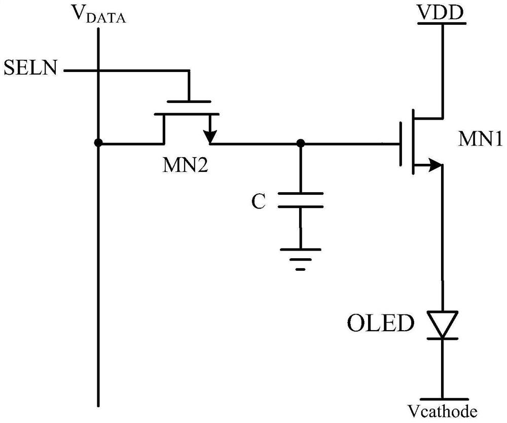
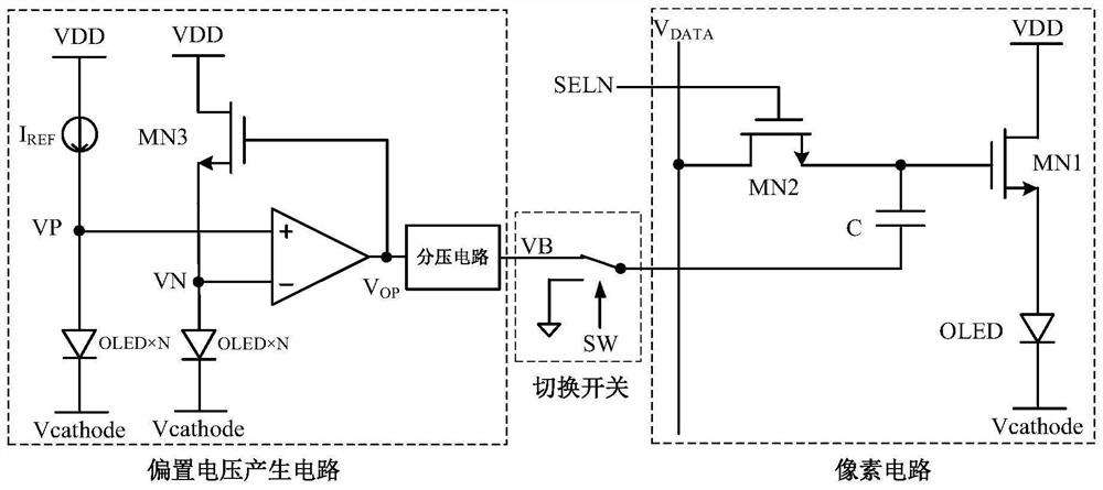
[0028] as attached figure 2 As shown, in one embodiment of the present invention, an image display device includes a pixel circuit, a switching switch, and a bias voltage generation circuit connected in sequence, wherein the driving transistor MN1, the switching transistor MN2, and the bias voltage generation circuit in the pixel circuit The adjustment tubes MN3 in the circuit are all N-type MOS tubes; the bias voltage generation circuit is used to generate a bias voltage VB, the input terminals of the switch are respectively connected to GND and the bias voltage VB, and the output terminals are connected to the pixel circuit , used to switch GND and bias voltage VB, the input of the pixel circuit is the data signal V DATA , the gate is connected to the row scanning signal...


PUM


Abstract

The invention discloses an image display device and a display method thereof. The device comprises a pixel circuit, a change-over switch and a bias voltage generation circuit which are connected in sequence, the bias voltage generating circuit is used for generating bias voltage VB, the input end of the change-over switch is connected with GND and the bias voltage VB, the output end of the change-over switch is connected with the pixel circuit and used for switching the GND and the bias voltage VB, the input end of the pixel circuit is a data signal VDATA, the grid electrode of the pixel circuit is connected with a line scanning signal SELN and the output end of the change-over switch, and the output end of the pixel circuit is connected with the anode of the OLED device. The bias voltage VB is used for controlling the OLED device to emit light, and the bias voltage VB is used for improving the brightness of the OLED device. According to the invention, an additional transistor does not need to be added in the pixel, and the maximum brightness of the OLED device can be improved under the condition that the power supply voltage is not changed.

Description

technical field [0001] The invention belongs to the technical field of micro-display driving circuits, and in particular relates to an image display device and a display method thereof. Background technique [0002] Silicon-based OLED (Organic Light Emitting Diode) microdisplay is a new type of microdisplay technology, which realizes the combination of display technology and silicon-based integrated circuit technology. Compared with other microdisplay technologies, silicon-based OLED microdisplay devices have the advantages of active light emission, high contrast, fast response, and high resolution, and are widely used in helmet display products and smart wearable products. [0003] figure 1 It is a 2T1C pixel circuit composed of a traditional N-type MOS tube used in silicon-based OLED micro-display chips, where MN1 is a drive tube, MN2 is a switch tube, and C is a capacitor. Data voltage V DATA The maximum voltage value of the switch tube MN2 can be close to the power su...

Claims


Application Information

Patent Timeline
Patent Type & Authority Applications(China)
IPC IPC(8): G09G3/3225
CPCG09G3/3225G09G2320/041G09G2320/043
Inventor 陈啟宏秦昌兵张白雪张叶明周海涛杨建兵
Owner NANJING GUOZHAO OPTOELECTRONICS TECH CO LTD
Why Eureka
Try Eureka