
Compact half-mode substrate integrated waveguide balance filter

A half-mode substrate integration, balanced filter technology, applied in waveguide-type devices, circuits, electrical components, etc., can solve problems such as narrow operating bandwidth, limited application, energy leakage, etc., to solve the effect of excessive volume

Active Publication Date: 2022-03-11
SHANGHAI JIAO TONG UNIV
View PDF8 Cites 0 Cited by
  • Summary
  • Abstract
  • Description
  • Claims
  • Application Information

AI Technical Summary

Problems solved by technology

So far, balanced filters based on various planar transmission line structures such as microstrip lines have been proposed one after another. However, the above transmission line structures are all open structures, and there is an energy leakage problem.
[0003] SIW (Substrate Integrated Waveguide, substrate integrated waveguide) is used in the design of balanced filters because of its excellent characteristics of low loss, low crosstalk, easy integration with planar microwave circuits, and high power capacity. However, the substrate integrated waveguide The cut-off frequency is related to the lateral size, which limits its application in compact microwave circuits
Subsequently, balanced filters based on variant structures of various SIWs were successively proposed, among which the balanced filters based on HMSIW (Half-mode Substrate Integrated Waveguide) and QMSIW (Quarter-mode Substrate Integrated Waveguide) were compared with those based on The balanced filter designed by SIW can reduce the lateral size, but its operating bandwidth is still narrow. In these designs, only the reduction of the lateral size of the SIW is focused.

Method used


Image

  • Compact half-mode substrate integrated waveguide balance filter
  • Compact half-mode substrate integrated waveguide balance filter
  • Compact half-mode substrate integrated waveguide balance filter

Examples


Embodiment 1

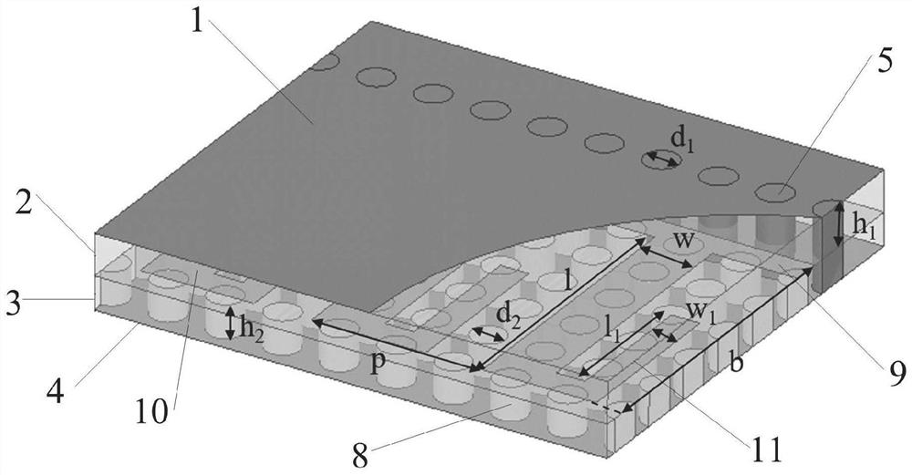
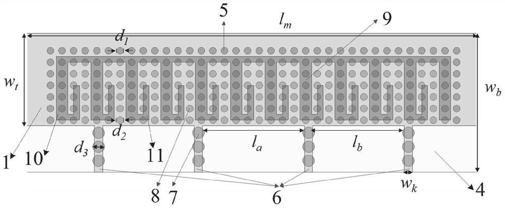
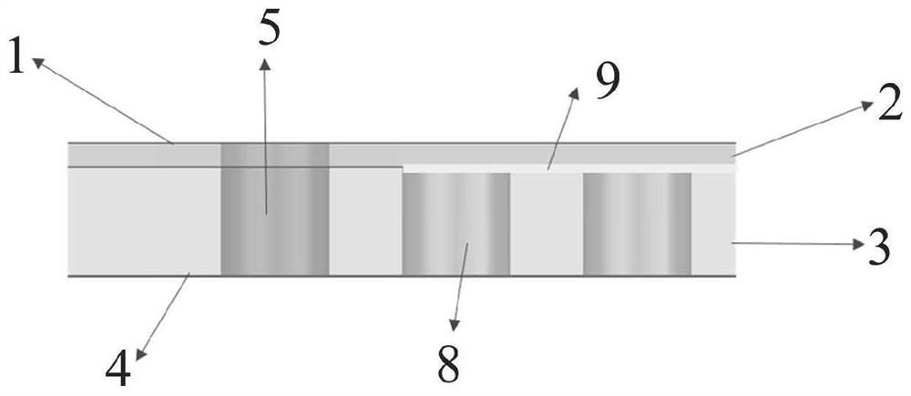
[0026] This embodiment is used to provide a compact half-mode substrate-integrated waveguide balanced filter. The balanced filter includes a half-mode substrate-integrated waveguide, a metal blind hole array and an artificial surface plasmon structure. Both the metal blind hole array and the artificial surface plasmon structure are located in the dielectric substrate of the half-mode substrate integrated waveguide, and the metal blind hole array is located in the space surrounded by the metal vias of the half-mode substrate integrated waveguide. The surface plasmon structure is located above the metal blind hole array, and the artificial surface plasmon structure is a subwavelength planar periodic groove structure.

[0027] In this embodiment, by introducing a metal blind hole array into the half-mode substrate integrated waveguide and etching a sub-wavelength artificial surface plasmon structure above the metal blind hole array, the slow wave of the half-mode substrate integra...


PUM

PropertyMeasurementUnit
lengthaaaaaaaaaa
widthaaaaaaaaaa
widthaaaaaaaaaa

Abstract

The invention relates to a compact half-mode substrate integrated waveguide balance filter which comprises a half-mode substrate integrated waveguide, a metal blind hole array and an artificial surface plasmon structure. The metal blind hole array and the artificial surface plasmon structure are both located in a dielectric substrate of the half-mode substrate integrated waveguide, the metal blind hole array is located in a space defined by the metal via holes, and the artificial surface plasmon structure is located above the metal blind hole array. According to the invention, the metal blind hole array is introduced into the half-mode substrate integrated waveguide, and the artificial surface plasmon structure is etched above the metal blind hole array, thereby achieving the regulation and control of the slow wave characteristics of the half-mode substrate integrated waveguide. The problems that a half-mode substrate integrated waveguide balance filter is too large in size, the compactness is not high when a microwave circuit is integrated, and the out-of-band characteristic is poor are solved, and miniaturization of the balance filter structure and the good out-of-band rejection characteristic are achieved.

Description

technical field [0001] The invention relates to the technical field of microwave communication, in particular to a compact half-mode substrate integrated waveguide balanced filter loaded with artificial surface plasmons and having excellent out-of-band characteristics. Background technique [0002] With the rapid development of modern communication technology, balanced filters play a key role in wireless communication due to their advantages of strong anti-interference ability and easy integration with other balanced circuits and antennas. A well-designed balanced filter means that it can suppress common-mode (CM) signals while responding to differential-mode (DM) signals within a certain frequency range. The performance of a balanced filter largely depends on the condition that does not affect the DM signal. Next, the inhibitory capacity of CM signaling. So far, balanced filters based on a variety of planar transmission line structures such as microstrip lines have been pr...

Claims


Application Information

Patent Timeline
Patent Type & Authority Applications(China)
IPC IPC(8): H01P1/212H01P1/20
CPCH01P1/212H01P1/2002
Inventor 李晓春朱宏彬纪磊毛军发
Owner SHANGHAI JIAO TONG UNIV
Learn More