Supercharge Your Innovation With Domain-Expert AI Agents!

Probe station

A technology of probe station and probe card, which is applied in the field of probe station, can solve the problems of lower contact accuracy, long time, vibration and vibration, etc., and achieve the goal of improving contact accuracy, reducing test delay time, and reducing vibration and vibration Effect

Pending Publication Date: 2022-03-29
SEMES CO LTD
View PDF20 Cites 0 Cited by
  • Summary
  • Abstract
  • Description
  • Claims
  • Application Information

AI Technical Summary

Problems solved by technology

However, when the movement of the upper camera unit is stopped by the stopper member, shock and vibration due to collision may occur, and since it takes a considerable time to remove the vibration, the test process for the substrate may be greatly delayed
In addition, the internal structure of the probe station may be slightly deformed by impact and vibration, and thus the contact accuracy between the substrate and the probe card may be reduced

Method used


Image

  • Probe station
  • Probe station
  • Probe station

Examples


Embodiment Construction

[0039] Hereinafter, embodiments of the present invention are described in more detail with reference to the accompanying drawings. However, the present invention is not limited to the embodiments described below and can be implemented in various other forms. The following examples are not intended to completely complete the present invention, but rather to fully convey the scope of the present invention to those skilled in the art.

[0040] In the specification, when a component is referred to as being "on" or "connected to" another component or layer, it can be directly located on, directly connected to, another component or layer, Or there may also be intermediate components or layers. In contrast, it will be understood that when a component is referred to as being directly on or connected to another component or layer, it means that there are no intervening components present. Also, although terms like first, second, and third are used to describe various regions and laye...


PUM


Abstract

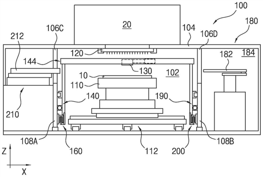
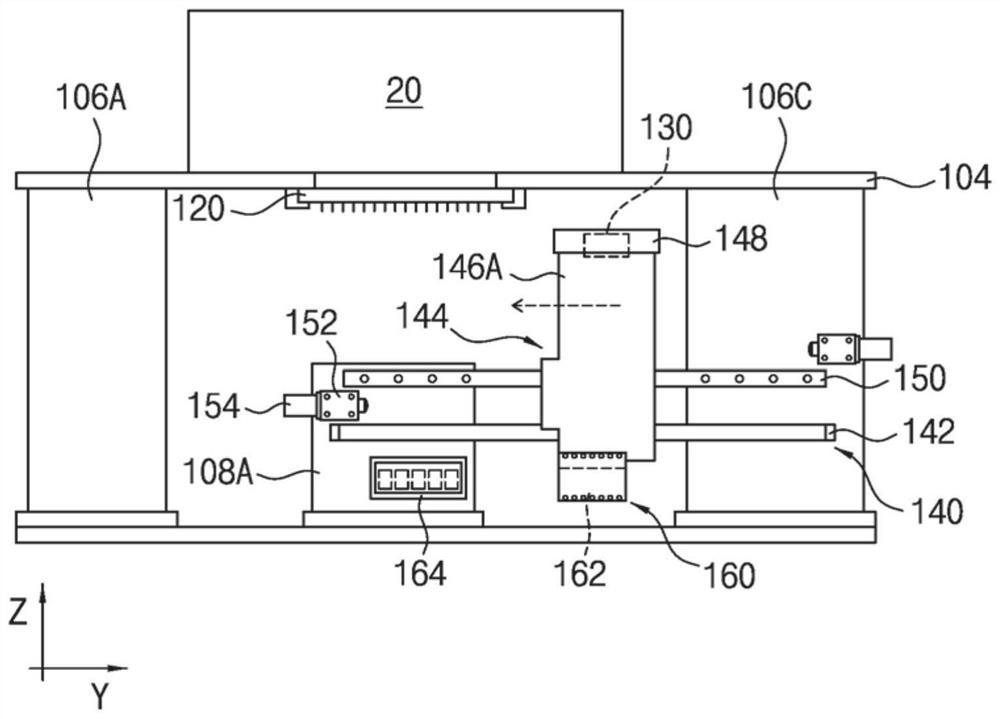
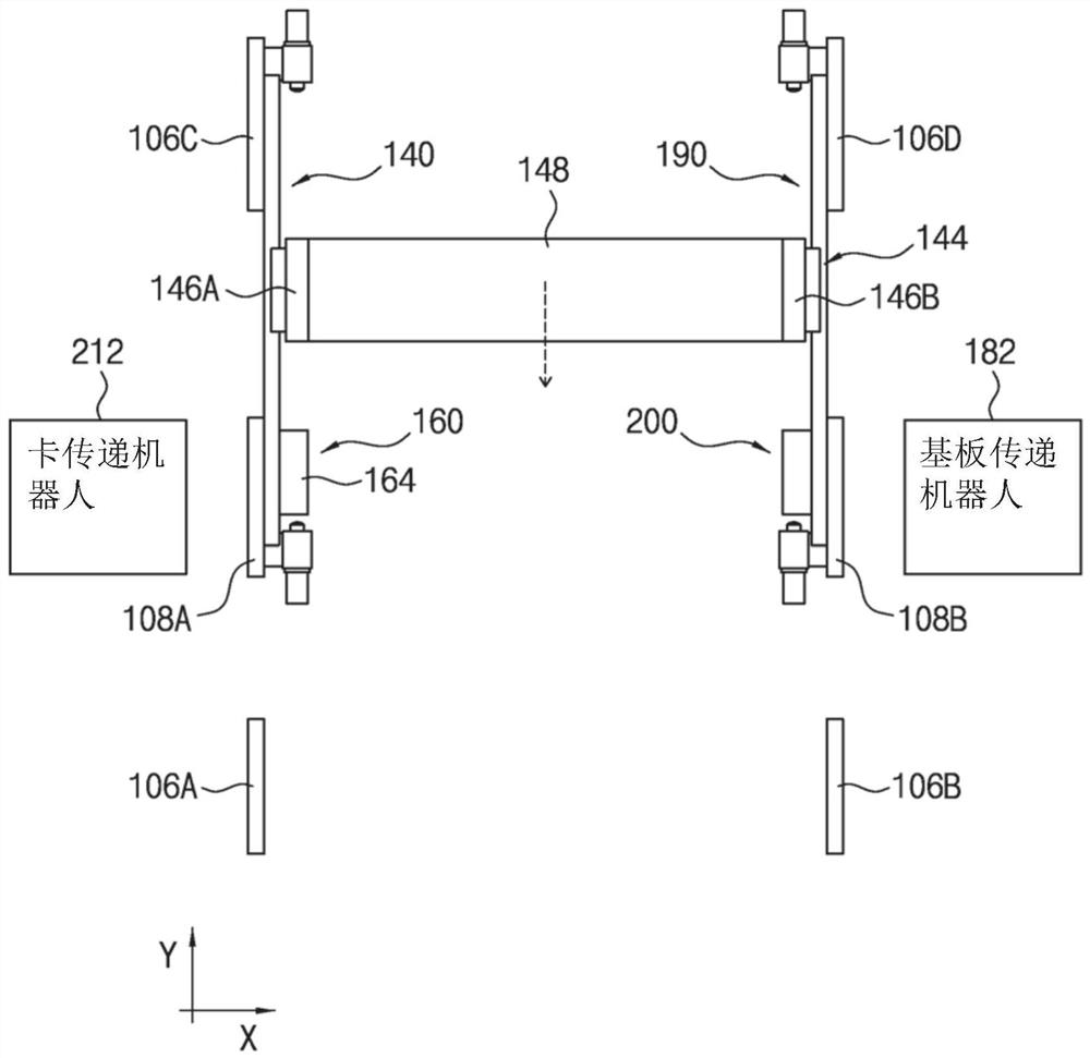
A probe station includes a chuck configured to support a substrate; a probe card disposed above the chuck and configured to electrically test a semiconductor device formed on the substrate; a camera unit disposed above the chuck and configured to image the substrate; and a camera driving member configured to move the camera unit in a horizontal direction. The camera driving member includes a braking unit for stopping the camera unit at a predetermined position using an eddy current braking force.

Description

technical field [0001] The invention relates to a probe station. More particularly, the present invention relates to a probe station for electrically testing a semiconductor device formed on a substrate using a probe card. Background technique [0002] A semiconductor device can be formed on a substrate, such as a silicon wafer, by repeatedly performing a series of manufacturing processes. For example, in order to manufacture a semiconductor device, various manufacturing processes may be performed on a wafer, such as a deposition process for forming thin layers on the wafer, an etching process for patterning thin layers to form circuits, flattening thin layers Planarized process, etc. [0003] After the semiconductor device is formed, an electrical test process for checking electrical characteristics of the semiconductor device may be performed. The test process may be performed by a probe station including a probe card having a plurality of probes, and a test head that s...

Claims


Application Information

Patent Timeline
Patent Type & Authority Applications(China)
IPC IPC(8): G01R1/073G01R31/26G01B11/00
CPCG01R1/07307G01R31/2601G01B11/00G01R31/2887G01R31/2893G01R31/2889G03B17/56H01F7/0273H04N23/57H04N23/695
Inventor 李赫柱
Owner SEMES CO LTD
Features
  • R&D
  • Intellectual Property
  • Life Sciences
  • Materials
  • Tech Scout
  • Unparalleled Data Quality
  • Higher Quality Content
  • 60% Fewer Hallucinations
Learn More