Display substrate and display device

A display substrate and substrate technology, applied to static indicators, instruments, electrical components, etc., can solve the problems of OLED current change, poor uniformity of light emission, uneven light emission of the display panel, etc., and achieve the effect of improving output characteristics

Pending Publication Date: 2022-03-29
BOE TECH GRP CO LTD
View PDF0 Cites 1 Cited by
  • Summary
  • Abstract
  • Description
  • Claims
  • Application Information

AI Technical Summary

Problems solved by technology

In the existing display panel, there is a phenomenon that the display panel does not emit light uniformly, that is, the uniformity of light emission is poor
For example, in OLED display panels, due to uncontrollable factors such as TFT and OLED light-emitting devices, such as process instability, parameter drift, and device aging, the OLED current changes, which in turn leads to uneven light emission of the display panel.

Method used


Image

  • Display substrate and display device
  • Display substrate and display device
  • Display substrate and display device

Examples


Embodiment Construction

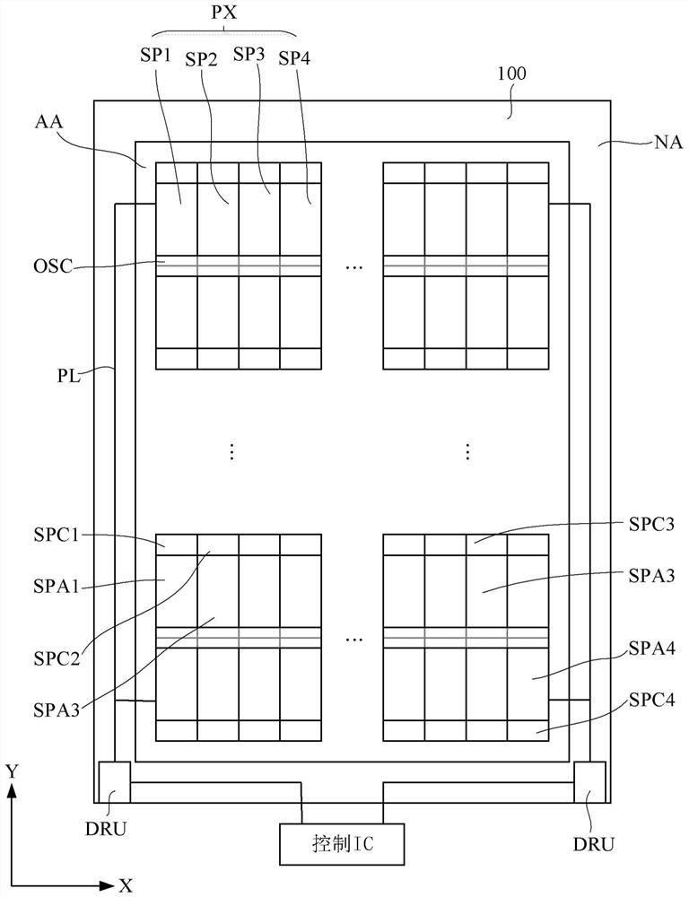
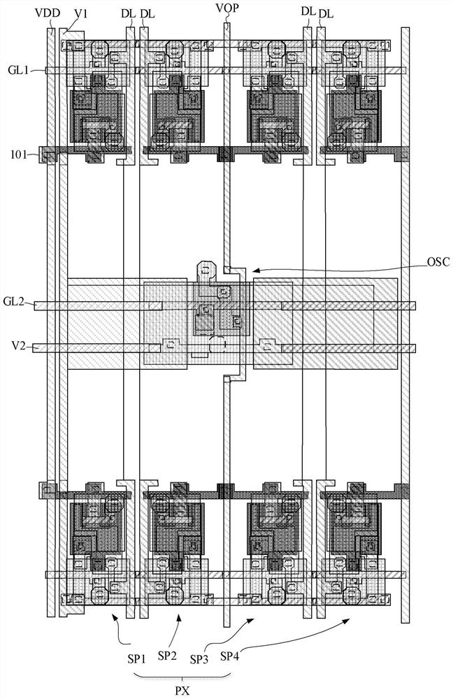
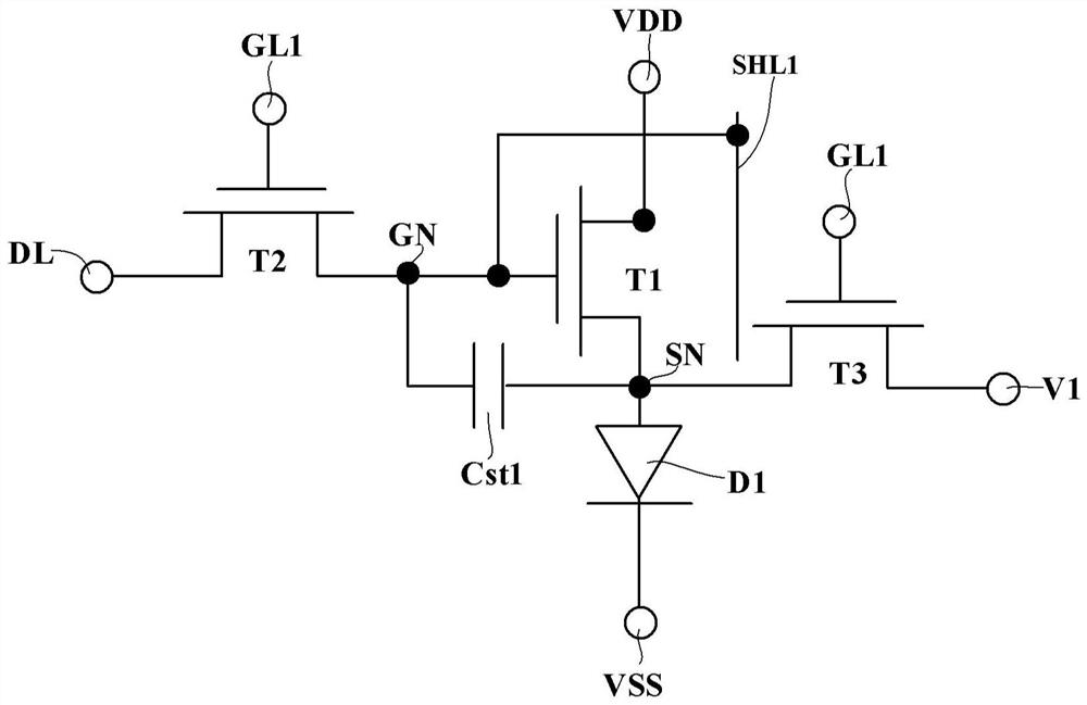
[0072] The technical solution of the present disclosure will be further described in detail through the following embodiments and in conjunction with the accompanying drawings. In the specification, the same or similar reference numerals designate the same or similar components. The following description of the embodiments of the present disclosure with reference to the accompanying drawings is intended to explain the general inventive concept of the present disclosure, and should not be construed as a limitation of the present disclosure.

[0073] In addition, in the following detailed description, for purposes of explanation, numerous specific details are set forth in order to provide a comprehensive understanding of the embodiments of the present disclosure. It may be evident, however, that one or more embodiments may be practiced without these specific details.

[0074] It will be understood that, although the terms first, second, etc. may be used herein to describe vario...


PUM


Abstract

The invention provides a display substrate and a display device. The display substrate comprises a substrate; the pixel units are arranged on the substrate, each pixel unit comprises a plurality of sub-pixels, and each sub-pixel comprises a light-emitting element and a pixel driving circuit used for driving the light-emitting element; the photosensitive circuit is arranged on the substrate; and the first conductive film layer is arranged on the substrate. The pixel driving circuit comprises a driving transistor, a grid electrode of the driving transistor is located on the side, away from the driving active layer, of the driving active layer, and the orthographic projection of the grid electrode of the driving transistor on the substrate and the orthographic projection of the driving active layer on the substrate are at least partially overlapped. The first conductive film layer at least comprises a first shading part, the first shading part is located between the substrate and the driving active layer, and the orthographic projection of the first shading part on the substrate and the orthographic projection of the driving active layer on the substrate are at least partially overlapped. The first light shielding portion is electrically connected to a gate of the driving transistor.

Description

technical field [0001] The present disclosure relates to the field of display technology, and in particular, to a display substrate and a display device. Background technique [0002] Luminous uniformity is one of the important indicators to measure the quality of display panels. In the existing display panel, there is a phenomenon that the display panel does not emit light uniformly, that is, the uniformity of light emission is poor. For example, in OLED display panels, due to uncontrollable factors such as TFT and OLED light-emitting devices such as process instability, parameter drift, and device aging, the OLED current changes, which in turn leads to uneven light emission of the display panel. Contents of the invention [0003] In order to solve at least one aspect of the above problems, embodiments of the present disclosure provide a display substrate and a display device. [0004] In one aspect, a display substrate is provided, the display substrate comprising: ...

Claims


Application Information

Patent Timeline
Patent Type & Authority Applications(China)
IPC IPC(8): H01L27/32G09G3/3233
CPCG09G3/3233H10K59/60H10K59/13H10K59/1213H10K59/1216H10K59/131H01L29/78633H10K50/865H01L27/124H01L27/1255
Inventor 韩影林奕呈王玲王国英张星高展徐攀
Owner BOE TECH GRP CO LTD
Why Eureka
Try Eureka