Two-dimensional material heterojunction field effect transistor, preparation method thereof and transistor array device

A heterojunction field effect, two-dimensional material technology, applied in the field of microelectronics, can solve the problems affecting transistor performance, two-dimensional material damage, low substrate utilization, etc., to avoid damage, low cost, good output characteristics and Effects of Transfer Features

Active Publication Date: 2016-12-07
科睿唯安(佛山)新能源科技有限公司
View PDF4 Cites 28 Cited by
  • Summary
  • Abstract
  • Description
  • Claims
  • Application Information

AI Technical Summary

Problems solved by technology

[0004] However, the main problem brought by the above two technologies is that only one device can be prepared on one substrate, and the utilization rate of the substrate is low.
More importantly, although photolithography can produce electrodes with regular patterns, it is easy to cause damage to the two-dimensional material during the process of evaporating metal electrodes, which will affect the performance of the transistor, and the cost is high, which is not conducive to application.

Method used


Image

  • Two-dimensional material heterojunction field effect transistor, preparation method thereof and transistor array device
  • Two-dimensional material heterojunction field effect transistor, preparation method thereof and transistor array device
  • Two-dimensional material heterojunction field effect transistor, preparation method thereof and transistor array device

Examples


preparation example Construction

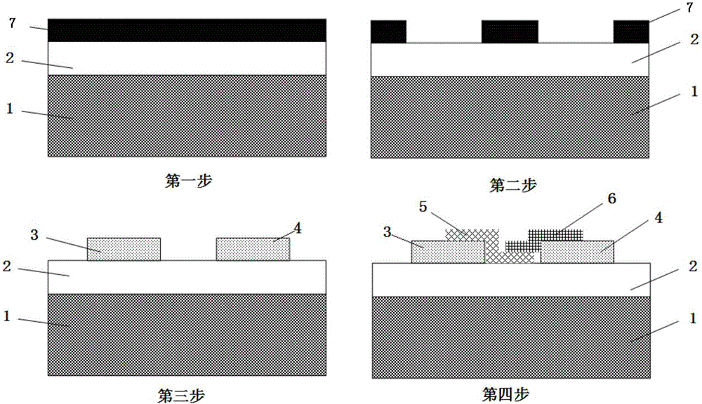
[0057] Correspondingly, the present invention provides a method for preparing a two-dimensional heterojunction field effect transistor, comprising the following steps:

[0058] 1) setting an insulating medium layer on the conductive substrate, and then spin-coating the photoresist on the insulating medium layer;

[0059] 2) making an electrode pattern mask on the insulating dielectric layer by photolithography and development;

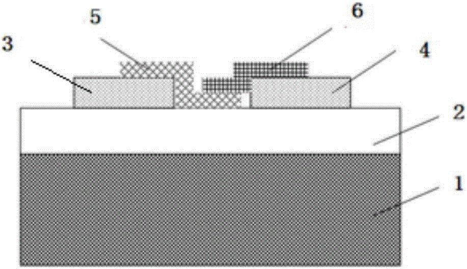
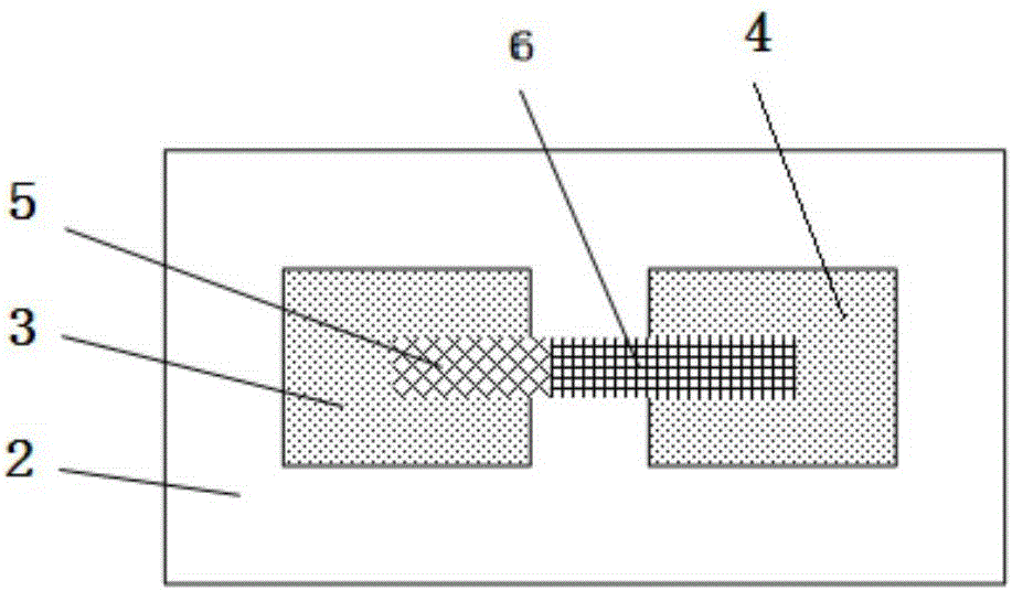
[0060] 3) Evaporating metal on the electrode pattern mask, then removing the photoresist on the insulating dielectric layer, forming a source electrode and a drain electrode at both ends thereof, between the source electrode and the drain electrode is the channel area;

[0061] 4) disposing a first two-dimensional material on the source electrode and the channel region connected thereto to form a first two-dimensional material layer, and then disposing a second two-dimensional material different from the first two-dimensional material on the source el...

Embodiment 1

[0076] Such as image 3 As shown, a method for preparing a two-dimensional material heterojunction field effect transistor comprises the following steps:

[0077] In the first step, a thermal oxidation method is used on the n-type conductive Si substrate 1 to obtain SiO with a thickness of 300nm 2 Insulation medium layer 2;

[0078] The 601 positive photoresist 7 was spin-coated on the insulating dielectric layer 2, the spin-coating time was 40 s, and the spin-coating speed was 4000 rpm.

[0079] In the second step, an electrode pattern mask is fabricated on the insulating dielectric layer 2 through photolithography and development; wherein, the photolithography time is 7s; the developer used is polyimide, and the development time is 35s.

[0080] In the third step, on the electrode pattern mask, utilize an electron beam evaporation evaporation deposition machine to successively evaporate (cavity vacuum degree is 10 -4 Pa, the coating rate is 0.1mm / s) a Ni layer with a thic...

Embodiment 2

[0086] This embodiment adopts the same transistor structure and fabrication process as in Embodiment 1, wherein the second two-dimensional material (MoSe 2 ) is replaced by the p-type second two-dimensional material (WSe 2 ), thus forming a MoS 2 / WSe 2 pn heterojunction field effect transistor, the physical picture is as follows Figure 8 as shown, Figure 8 is the MoS provided by Example 2 of the present invention 2 / WSe 2 Pn heterojunction field effect transistor physical map.

[0087] Using a probe station and a dual-channel SourceMeter, the MoS 2 / WSe 2 pn heterojunction field effect transistor for performance testing. See results Figure 9 with Figure 10 , Figure 9 is the MoS provided by Example 2 of the present invention 2 / WSe 2 I-V characteristic curve of pn heterojunction field effect transistor, Figure 10 is the MoS provided by Example 2 of the present invention 2 / WSe 2 Transfer curves of a pn heterojunction field effect transistor. from Figur...


PUM


Abstract

The invention provides a two-dimensional material heterojunction field effect transistor, a preparation method thereof and a transistor array device. The transistor comprises a conductive substrate, an insulating dielectric layer, a source electrode, a drain electrode, a first two-dimensional material layer and a second two-dimensional material layer, wherein the insulating dielectric layer is arranged on the conductive substrate; the source electrode and the drain electrode are arranged at two ends of the insulating dielectric layer respectively and a channel region is arranged between the source electrode and the drain electrode; the first two-dimensional material layer is arranged on the source electrode and the channel region connected with the source electrode; the second two-dimensional material layer is arranged on the drain electrode and one part of first two-dimensional material layer on the channel region; the first two-dimensional material layer is different from the second two-dimensional material layer in material; the first two-dimensional material layer, the second two-dimensional material layer, the source electrode and the drain electrode can form ohmic contact. The transistor provided by the invention has good properties of output characteristics and the like and is low in cost. The preparation method of the transistor provided by the invention is high in substrate utilization rate and high in preparation efficiency; the damage of metal evaporation to a two-dimensional material can be avoided; and the array device can also be prepared.

Description

technical field [0001] The invention relates to the technical field of microelectronics, in particular to a two-dimensional material heterojunction field effect transistor, a preparation method thereof and a transistor array device. Background technique [0002] As the earliest discovered two-dimensional nanomaterial, graphene has great application potential in the field of nano-optoelectronics due to its unique physical and chemical properties, and has attracted a lot of attention and research in recent years. However, the zero-bandgap property of graphene limits its wide practical application in the field of nanoelectronics. Although people use various methods to open its band gap, the opened band gap is still very small and has little effect. In recent years, as an alternative to graphene, two-dimensional transition metal chalcogenides (TMDs) are gradually emerging. They have a certain size band gap (1-3eV) and exhibit excellent optoelectronic properties. For example, b...

Claims


Application Information

Patent Timeline
Patent Type & Authority Applications(China)
IPC IPC(8): H01L29/778H01L29/417H01L29/10H01L21/336
CPCH01L29/1033H01L29/41725H01L29/66242H01L29/7787H01L29/7789
Inventor 杨亿斌招瑜肖也牟中飞李京波
Owner 科睿唯安(佛山)新能源科技有限公司
Why Eureka
Try Eureka