Photovoltaic device

a photovoltaic device and photovoltaic technology, applied in the direction of semiconductor/solid-state device details, radiation control devices, instruments, etc., can solve the problems of disadvantageously difficult to improve the output characteristics of the photovoltaic device, and no sufficient countermeasure for suppressing the recombination of carriers, etc., to achieve the effect of improving the output characteristics

Active Publication Date: 2011-01-04
SANYO ELECTRIC CO LTD
View PDF59 Cites 28 Cited by
  • Summary
  • Abstract
  • Description
  • Claims
  • Application Information

AI Technical Summary

Benefits of technology

[0007]The present invention has been proposed in order to solve the aforementioned problem, and an object thereof is to provide a photovoltaic device capable of improving output characteristics.

Problems solved by technology

However, the aforementioned photovoltaic device disclosed in Japanese Patent Laying-Open No. 2001-345463 has no sufficient countermeasure for suppressing recombination of carriers caused by dangling bonds forming defects in the substantially intrinsic amorphous silicon layer when carriers formed in the single-crystalline silicon substrate are moved into the p-type amorphous silicon layer through the substantially intrinsic amorphous silicon layer.
Therefore, photo-produced carriers disappear in the substantially intrinsic amorphous silicon layer due to recombination, and hence it is disadvantageously difficult to improve the output characteristics of the photovoltaic device.

Method used


Image

  • Photovoltaic device
  • Photovoltaic device
  • Photovoltaic device

Examples


Embodiment Construction

[0035]An embodiment of the present invention is now described with reference to the drawings.

[0036]The structure of a photovoltaic device according to the embodiment is described with reference to FIG. 1.

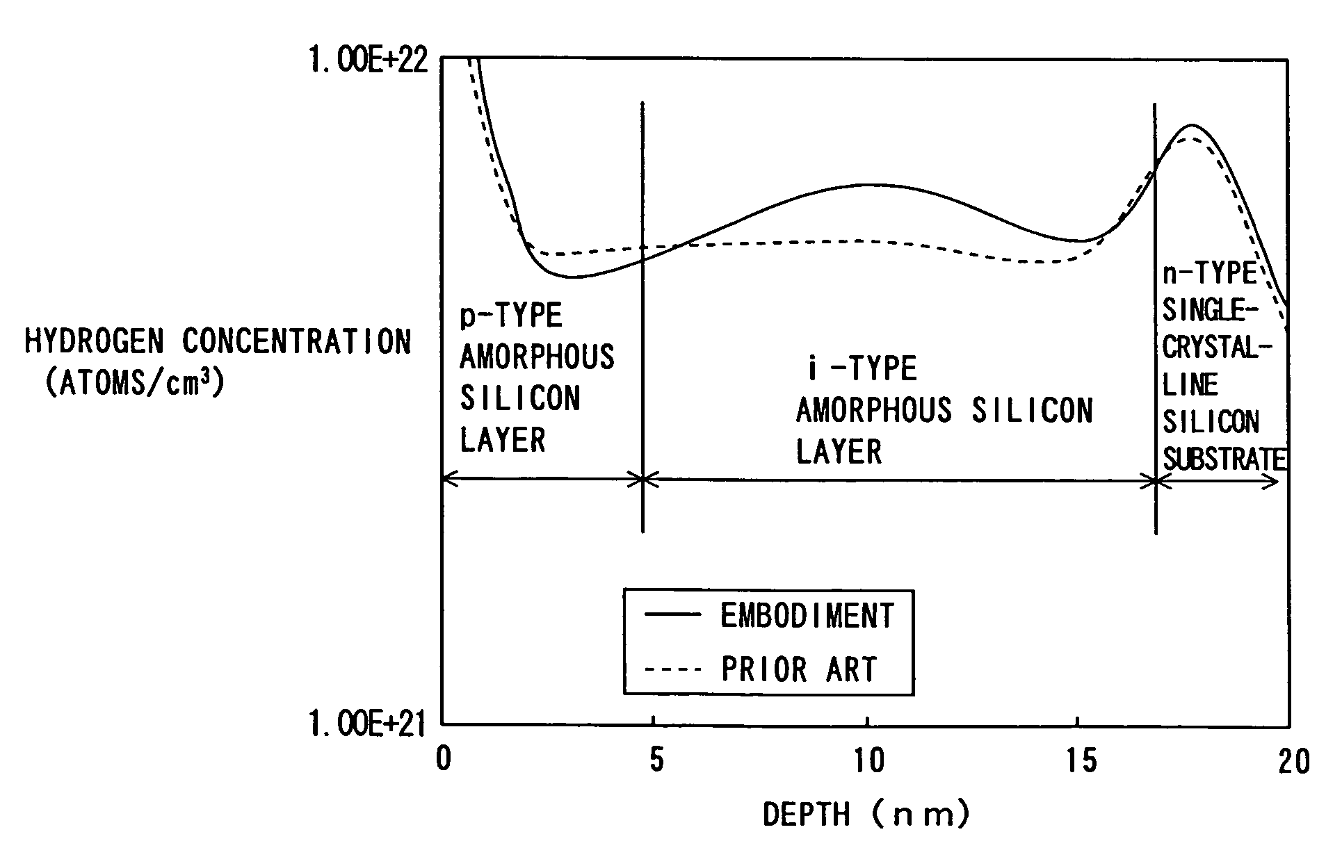
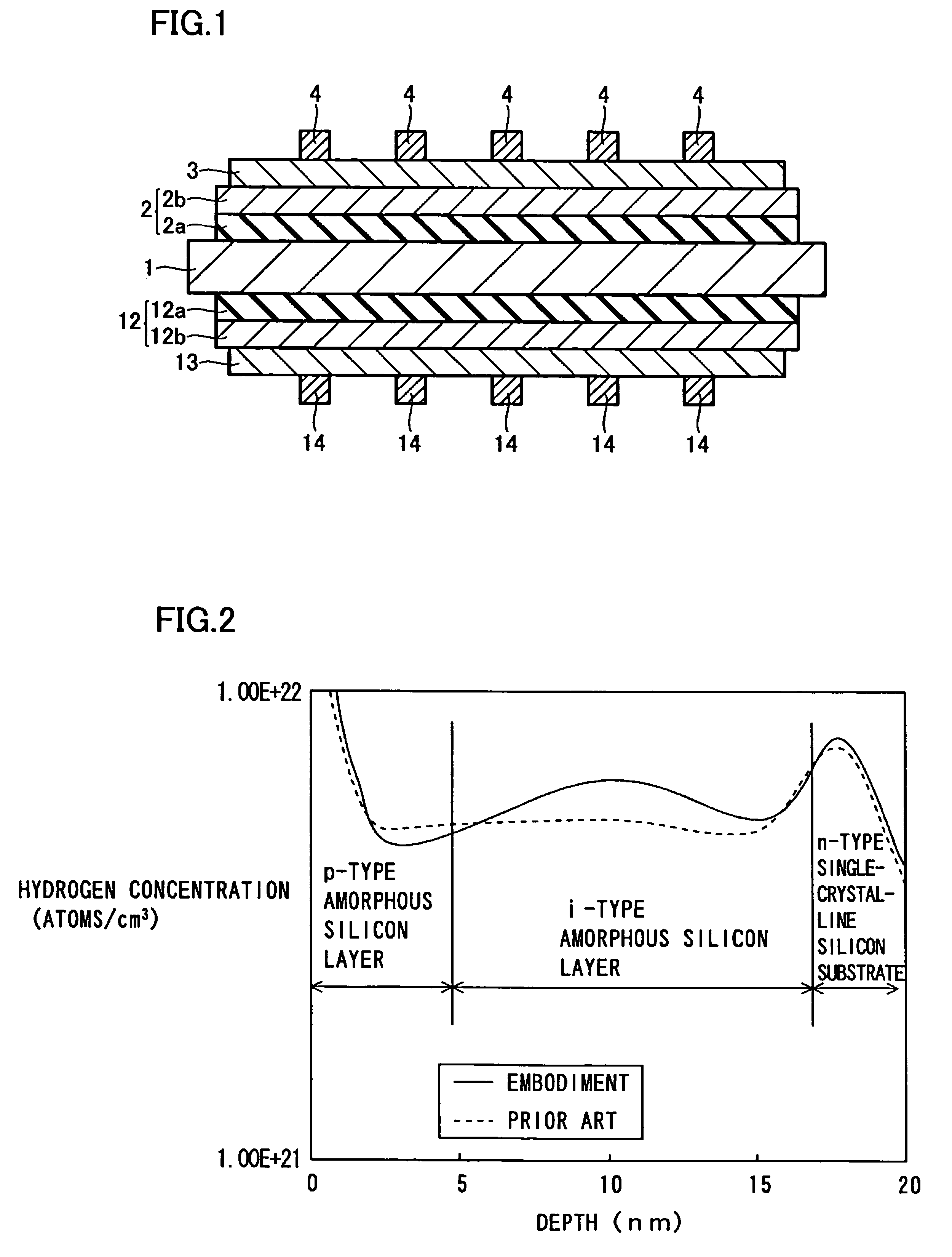
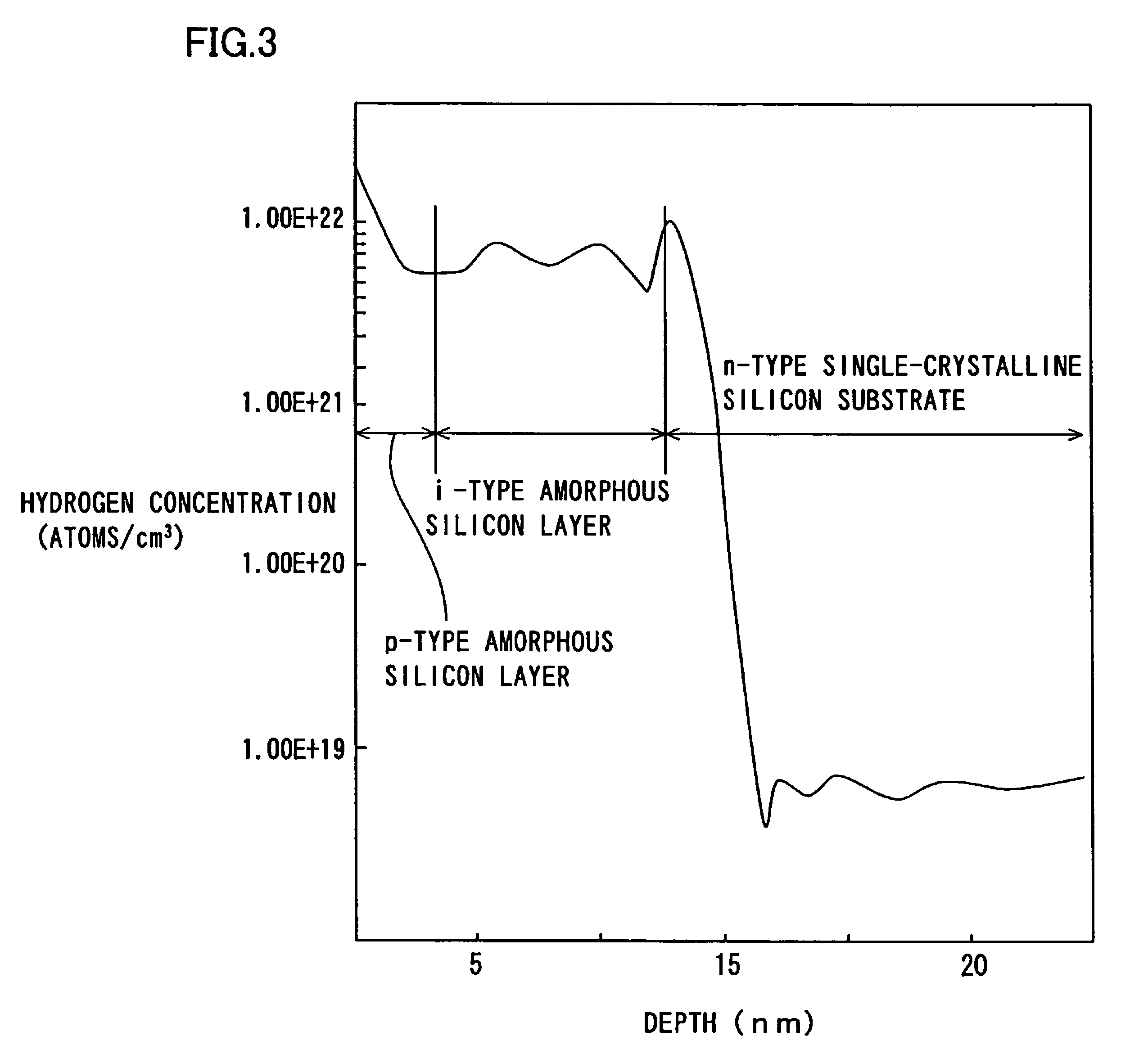
[0037]In the photovoltaic device according to the embodiment, an amorphous silicon layer 2, a front electrode 3 of ITO (indium tin oxide) having a thickness of about 70 nm to about 100 nm and a collector 4 of silver having a thickness of several 10 μm are successively formed on the upper surface of a hydrotreated single-crystalline silicon substrate 1, as shown in FIG. 1. The amorphous silicon layer 2 is constituted of a substantially intrinsic i-type amorphous silicon layer 2a having a small thickness of about 9 nm to about 13 nm formed on the upper surface of the n-type single-crystalline silicon substrate 1 and a p-type amorphous silicon layer 2b, doped with boron (B), having a thickness of about 2 nm to about 5 nm formed on the i-type amorphous silicon layer 2a. The i-type amorp...


PUM

PropertyMeasurementUnit
thicknessaaaaaaaaaa
thicknessaaaaaaaaaa
thicknessaaaaaaaaaa

Abstract

A photovoltaic device capable of improving output characteristics is provided. This photovoltaic device comprises a crystalline semiconductor member, a substantially intrinsic first amorphous semiconductor layer formed on the front surface of the crystalline semiconductor member and a first conductivity type second amorphous semiconductor layer formed on the front surface of the first amorphous semiconductor layer, and has a hydrogen concentration peak in the first amorphous semiconductor layer. Thus, the quantity of hydrogen atoms in the first amorphous semiconductor layer is so increased that the hydrogen atoms increased in quantity can be bonded to dangling bonds of silicon atoms forming defects in the first amorphous semiconductor layer for inactivating the dangling bonds.

Description

BACKGROUND OF THE INVENTION[0001]1. Field of the Invention[0002]The present invention relates to a photovoltaic device, and more particularly, it relates to a photovoltaic device having amorphous semiconductor layers formed on a crystalline semiconductor member.[0003]2. Description of the Background Art[0004]In relation to a photovoltaic device prepared by forming a second conductivity type amorphous silicon layer on the front surface of a first conductivity type crystalline silicon substrate thereby forming a p-n junction, a technique of inserting a substantially intrinsic amorphous silicon layer between the first conductivity type crystalline silicon substrate and the second conductivity type amorphous silicon layer thereby improving junction characteristics is known in general. For example, Japanese Patent Laying-Open No. 2001-345463 discloses this technique.[0005]The aforementioned Japanese Patent Laying-Open No. 2001-345463 discloses a photovoltaic device prepared by successive...

Claims


Application Information

Patent Timeline
Patent Type & Authority Patents(United States)
IPC IPC(8): H01L31/00H01L31/04H01L31/20H01L31/075H01L27/146H01L31/0376H01L31/06H01L31/072H01L31/0745H01L31/0747H01L31/076H01L31/18
CPCH01L31/03762H01L31/0745H01L31/076H01L31/202Y10T428/24917Y02E10/548Y02E10/547H01L31/0747Y02P70/50
Inventor TERAKAWA, AKIRAASAUMI, TOSHIO
Owner SANYO ELECTRIC CO LTD
Why Eureka
Try Eureka