Label

A label and slot technology, applied in the field of labels, can solve the problem of inability to read state changes with high precision, and achieve the effect of improving the SN ratio

Pending Publication Date: 2022-03-29
KONICA MINOLTA INC
View PDF9 Cites 0 Cited by
  • Summary
  • Abstract
  • Description
  • Claims
  • Application Information

AI Technical Summary

Problems solved by technology

Therefore, in the tag reader, there is a problem that the identification information attached to the

Method used


Image

  • Label
  • Label
  • Label

Examples


no. 2 Embodiment approach

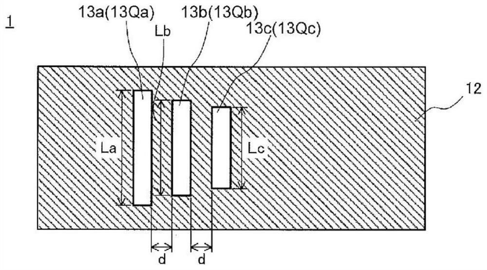
[0140] Next, refer to Figure 12A ~ Figure 16B , and the structure of the label 1 according to the second embodiment will be described. The tag 1 according to this embodiment is different from the first embodiment in that a resonant element is formed by a ring-shaped (and circular) slit instead of a rectangular slit. In addition, the description of the configuration common to the first embodiment is omitted.

[0141] Figure 12A and Figure 12B shows the structure of the tag 1 according to the present embodiment ( Figure 12A ) and the reflection characteristics of the label 1 according to this embodiment ( Figure 12B ) graph.

[0142] The label 1 according to the present embodiment includes a base material 11 and a conductive pattern layer 12 arranged on the base material 11 similarly to the first embodiment. In addition, three slits 13 f , 13 g , and 13 h are formed in the conductive pattern layer 12 . The slots 13f, 13g, and 13h constitute resonance elements 13Qf, 1...

no. 3 Embodiment approach

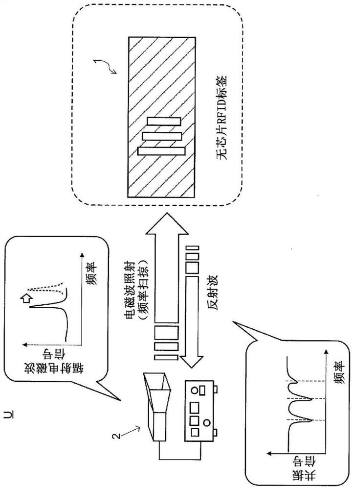
[0163] In the above-mentioned embodiment, the form which used the tag 1 as the identifier of the RFID system U was shown. However, the tag of the present invention can also be used as a chipless sensor tag (hereinafter simply referred to as "tag") of a state detection system that detects a state change of an object or environment in a non-contact manner (for example, refer to Patent Document 2).

[0164] Figure 17 It is a figure which shows an example of the structure of the state detection system Ux which concerns on this embodiment. Figure 18A and Figure 18B It is a figure which shows an example of the structure of the tag 1x concerning this embodiment. also, Figure 18A represents the basic structure of label 1x, Figure 18B Indicates a modified example of label 1x.

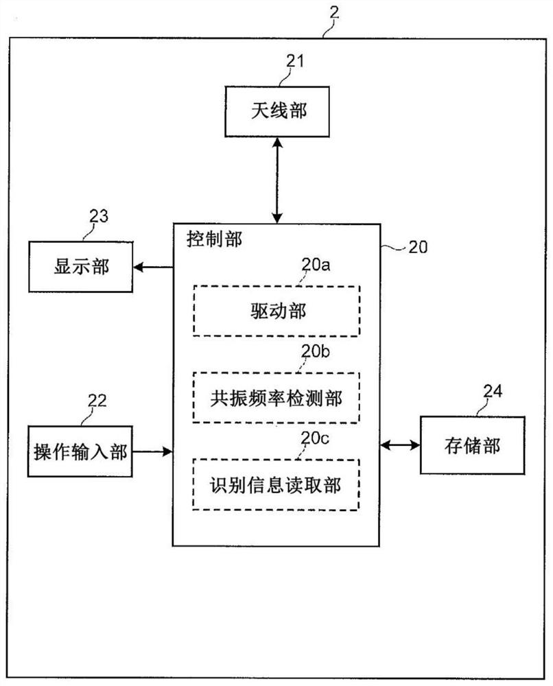
[0165] The state detection system Ux has a tag 1x and a tag reader 2x. The basic configurations of the tag 1x and the tag reader 2x are the same as those of the tag 1 and the tag reader 2 according to...


PUM


Abstract

A label which represents the properties thereof by means of electromagnetic wave reflection characteristics, and which is provided with: a base material (11); and a conductor pattern layer (12) formed on the base material (11) and having first and second slits (13a, 13b) disposed adjacent to each other, the first slit (13a) constituting a first resonance element (13Qa) having a resonance frequency at a first frequency, the second slit (13b) constituting a second resonance element (13Qb) having a resonance frequency at a second frequency higher than the first frequency, and the conductor pattern layer (12) being formed on the base material (11) when irradiated with electromagnetic waves. The Q value of the formant exhibited at the first frequency is higher than the Q value of the formant exhibited at the first frequency when the resonance structure of the tag is individually configured by the first slit (13a).

Description

technical field [0001] This disclosure relates to tags. Background technique [0002] In recent years, an RFID system using tags called "chipless RFID tags" has attracted attention as a technology to replace barcodes and electronic tags with built-in IC chips. [0003] A chipless RFID tag does not have an integrated circuit in the tag, but constitutes identification information by reflection characteristics when it is irradiated with electromagnetic waves. In addition, in such an RFID system, the chipless RFID tag is irradiated with electromagnetic waves from the tag reader, and the tag reader detects the reflection characteristics of the chipless RFID tag, thereby reading the chipless RFID tag. identification information. [0004] As such a chipless RFID tag, for example, a tag is known in which a plurality of resonant elements having different resonance frequencies are formed on the base material of the tag, and identification information is expressed by a combination of...

Claims


Application Information

Patent Timeline
IPC IPC(8): G06K19/067H01Q15/14
CPCG06K19/067H01Q15/14H01Q13/106H01Q21/28H01Q1/2225G06K19/0672G06K19/0707G06K19/0723G06K19/07758
Inventor 石渡拓己高桥伸明新井贤司波木井健
Owner KONICA MINOLTA INC
Why Eureka
Try Eureka