Solid-state image pickup device and camera using the same solid-state image pickup device

A solid-state imaging device and pixel technology, which is applied in image communication, color TV components, and TV system components, etc., can solve problems such as reduction, and achieve the effect of small time deviation and easy design.

Inactive Publication Date: 2005-11-16
CANON KK
View PDF4 Cites 0 Cited by
  • Summary
  • Abstract
  • Description
  • Claims
  • Application Information

AI Technical Summary

Problems solved by technology

That is, the signal voltage read from the pixel is significantly reduced by signal division in the signal transfer path, and thus is affected by thermal noise on the transfer line.

Method used


Image

  • Solid-state image pickup device and camera using the same solid-state image pickup device
  • Solid-state image pickup device and camera using the same solid-state image pickup device
  • Solid-state image pickup device and camera using the same solid-state image pickup device

Examples


Embodiment approach 1

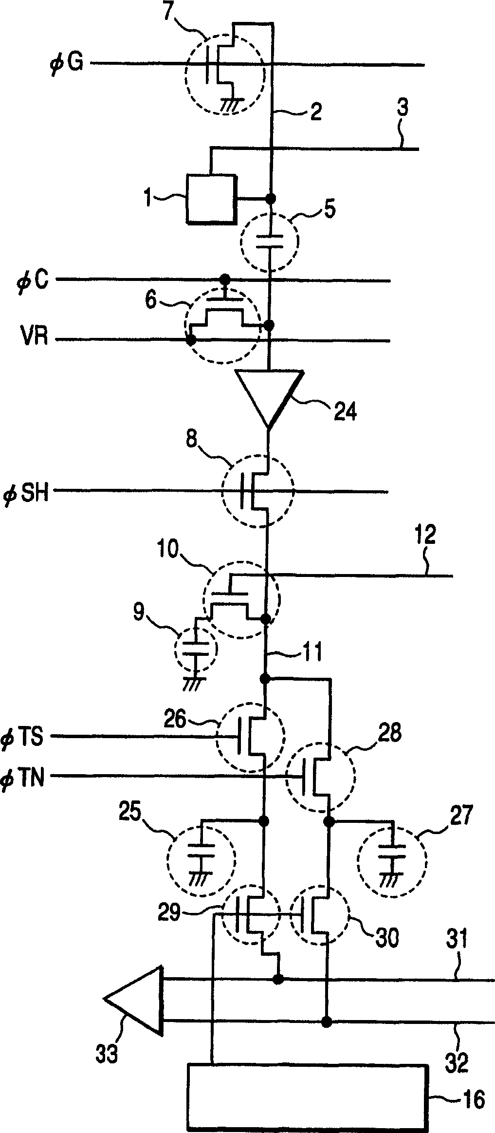
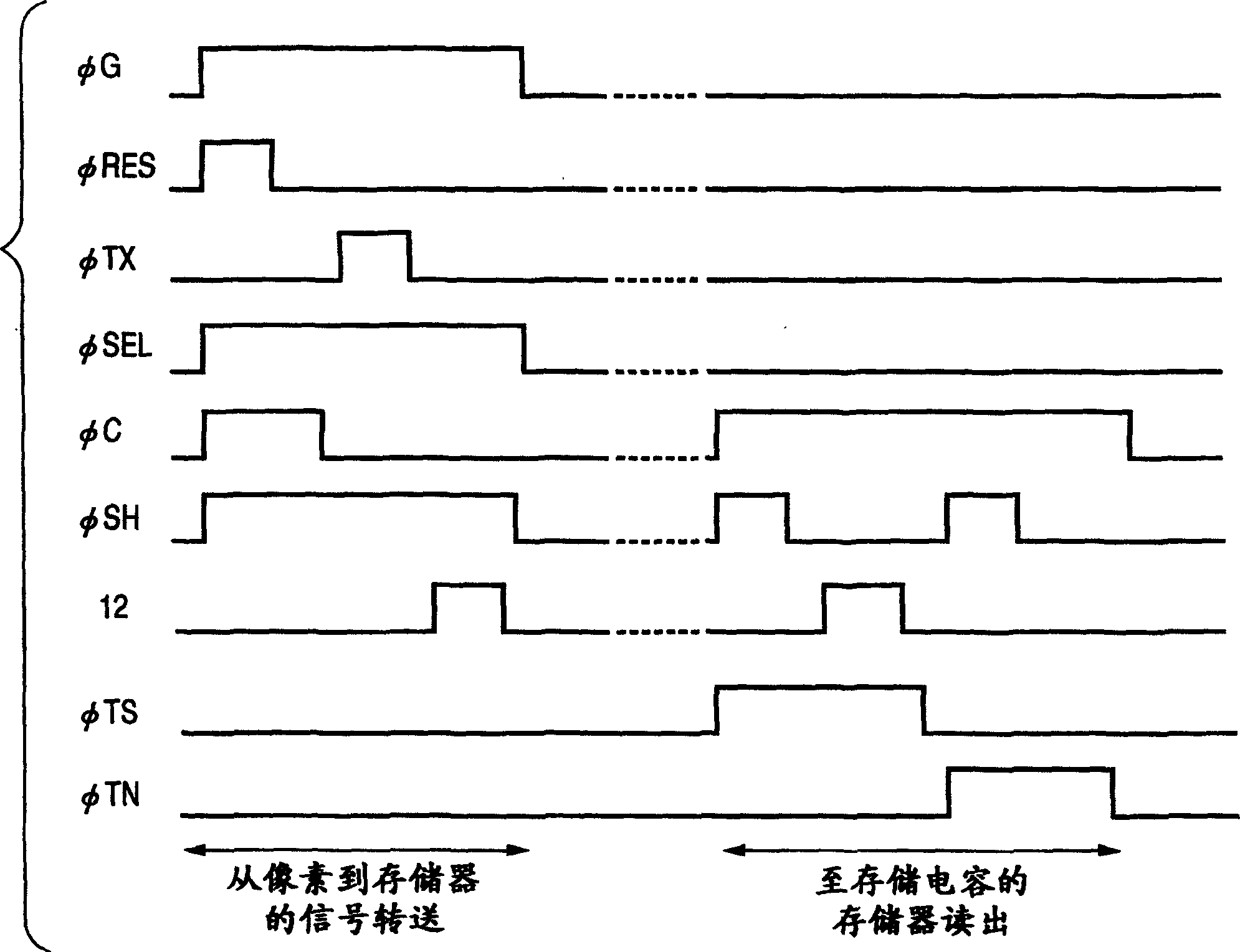
[0028] figure 1 It is a circuit diagram of a sensor along a signal line from a pixel to a sensor output in Embodiment 1 of the present invention. Here, for the sake of simplicity, one pixel, one storage unit, and one column of readout devices are shown, but in fact it is as follows Figure 8 The pixels and memory cells shown are arranged in two dimensions, and a readout device is provided for each column. Also in Figure 8 3×3 pixels and storage units are shown in the figure for simple pixels and storage units, but the number of pixels and storage units is set according to needs, and the number of storage units can also be less than the number of pixels. For example, when signals from a plurality of pixels are added or thinned out and stored in storage units, the number of storage units may be less than the number of pixels, but of course the number of storage units corresponding to the number of pixels required to form an image is required number. For example, a memory uni...

Embodiment approach 2

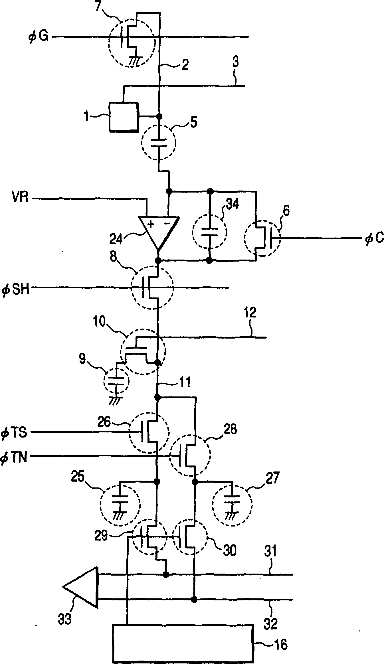
[0039] image 3 A circuit diagram of a sensor along a signal line from a pixel to an output sensor in Embodiment 2 of the present invention is shown. exist image 3 Among them, the column amplifier 24 is a feedback amplifier whose output is transmitted to the negative input terminal via the coupling capacitor 34 . Thus, the gain of the column amplifier 24 is determined by the ratio of the coupling capacitor 5 and the coupling capacitor 34 . The positive input terminal (+) is fixed at the clamp potential VR. The negative input terminal (-) is clamped at the clamp potential VR by applying the pulse φC to the clamp transistor 6 because the above-mentioned two input terminals are in a virtual short-circuit state. Thus, the pulse timing and figure 2 The pulse timings of Embodiment 1 shown are the same. But when image 3 The circuit in is more suitable for the present invention in that the coupling capacitor 5 used for clamping also serves to determine the gain of the column ...

Embodiment approach 3

[0041] Figure 4 A circuit diagram of a sensor along a signal line from a pixel to a sensor output in Embodiment 3 of the present invention is shown. In this figure, a memory with an amplification function in the cell is used. For example, as disclosed in US Pat. No. 5,805,429, an amplified analog memory cell already exists. exist Figure 4 Among them, the memory cell 35 is composed of an amplification transistor 36 , a memory selection transistor 37 , a write transistor 10 , and a memory cell capacitor 9 .

[0042] The current supply transistor 38 supplies a current so that the amplification transistor 36 operates as a source follower. In the third embodiment of the present invention, this amplified frame memory is used instead of the DRAM type memory used in the first and second embodiments.

[0043] Figure 5 It is a pulse timing chart showing the operation of the sensor according to Embodiment 3 of the present invention. according to Figure 4 , Figure 5 Describe ...


PUM


Abstract

The invention provides a solid-state image pickup device with little gap in operation timings of the pixels, providing a sensor output of a high S / N ratio. In a solid-state image pickup device provided with a photoelectric conversion pixel unit formed by an array of a plurality of pixels each containing at least a photoelectric conversion unit and a transistor for amplifying a signal from the photoelectric conversion unit, and memory units formed by an array of analog memory cells corresponding to at least a part of the pixels of the photoelectric conversion pixel unit, there are provided plural coupling capacitors respectively connected to plural output lines each of which is connected to a column of pixels, for clamping a signal from a pixel thereby eliminating a noise from the pixel, and plural amplifiers for amplifying a signal voltage from the coupling capacitor with a gain exceeding unity and outputting an amplified signal for writing into the analog memory cell.

Description

technical field [0001] The present invention relates to a solid-state imaging device and an imaging system, and in particular to an amplified solid-state imaging device and a camera provided with photoelectric conversion pixel units. The pixel is composed of transistors that transform the signal of the unit. Background technique [0002] Conventionally, as a solid-state imaging device, a CCD is often used from the viewpoint of a good SN ratio. However, on the other hand, a so-called amplifying solid-state imaging device has been developed, which has the advantages of easy usage and low power consumption. The so-called amplifying solid-state imaging device is a type in which signal charge accumulated in a light-receiving pixel is introduced into a control electrode of a transistor provided in a pixel unit, and an amplified signal is output from a main electrode. Specifically, there is an SIT-type image sensor using a SIT as an amplifier transistor (A. Yusa, J. Nishizawa et ...

Claims


Application Information

Patent Timeline
Patent Type & Authority Applications(China)
IPC IPC(8): H04N5/335H04N5/357H04N5/374H04N5/378
CPCH04N5/363H04N5/365H04N25/65H04N25/67
Inventor 篠原真人
Owner CANON KK
Why Eureka
Try Eureka