Method and apparatus for perforating printed circuit board

A technology for printed circuit boards and punching devices, which is applied in the direction of printed circuit manufacturing, printed circuits, electrical components, etc., can solve the problems of not being able to realize the high density of printed circuit boards, and achieve the improvement of SN ratio and increase Processing efficiency, high-quality processing effect

Inactive Publication Date: 2010-09-08
HITACHI SEIKO LTD
View PDF2 Cites 0 Cited by
  • Summary
  • Abstract
  • Description
  • Claims
  • Application Information

AI Technical Summary

Problems solved by technology

Therefore, the spacing between the holes cannot be narrowed, and the so-called high density of the printed circuit board cannot be realized by reducing the size of the printed circuit board.

Method used


Image

  • Method and apparatus for perforating printed circuit board
  • Method and apparatus for perforating printed circuit board
  • Method and apparatus for perforating printed circuit board

Examples


Embodiment 1

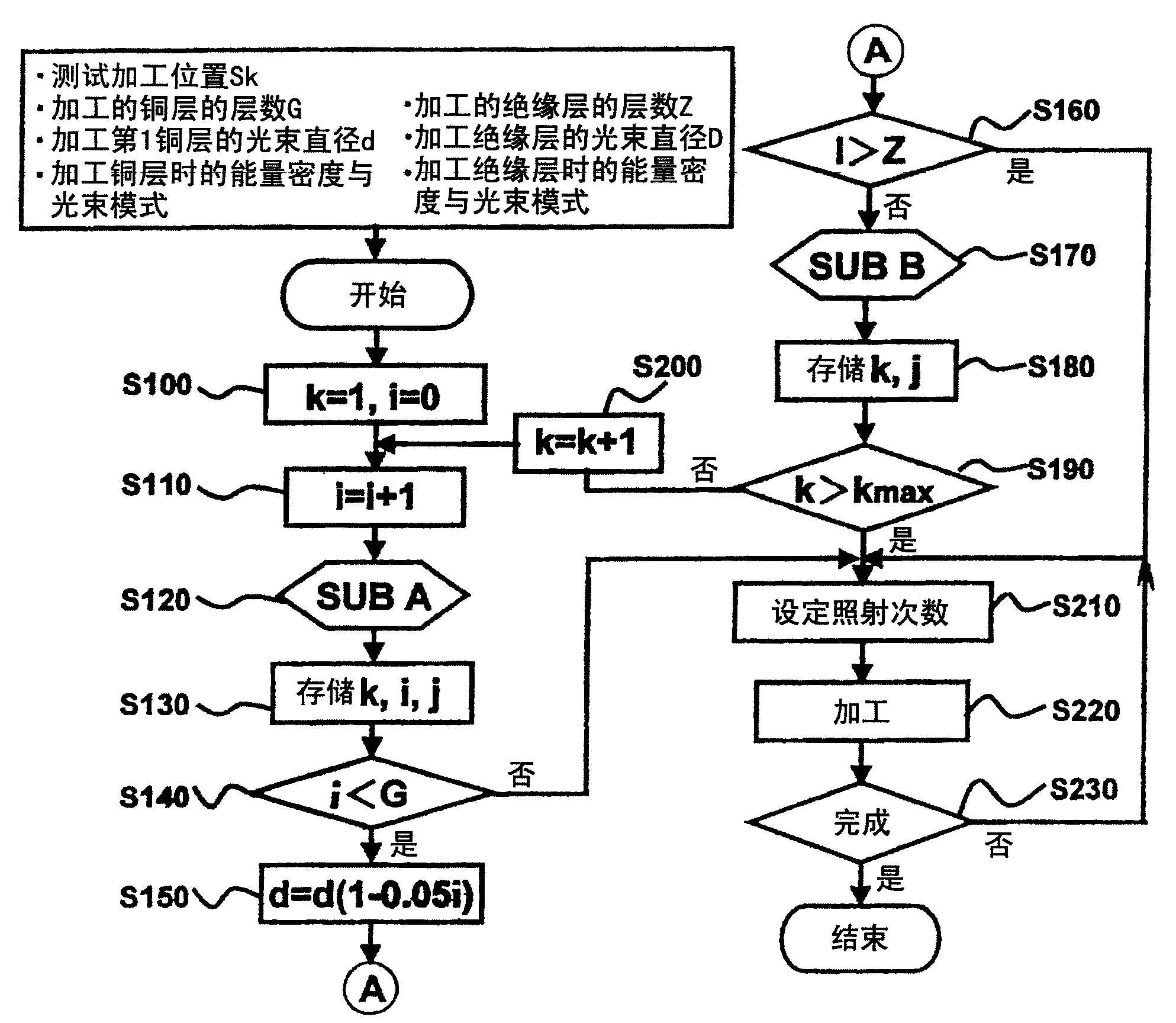
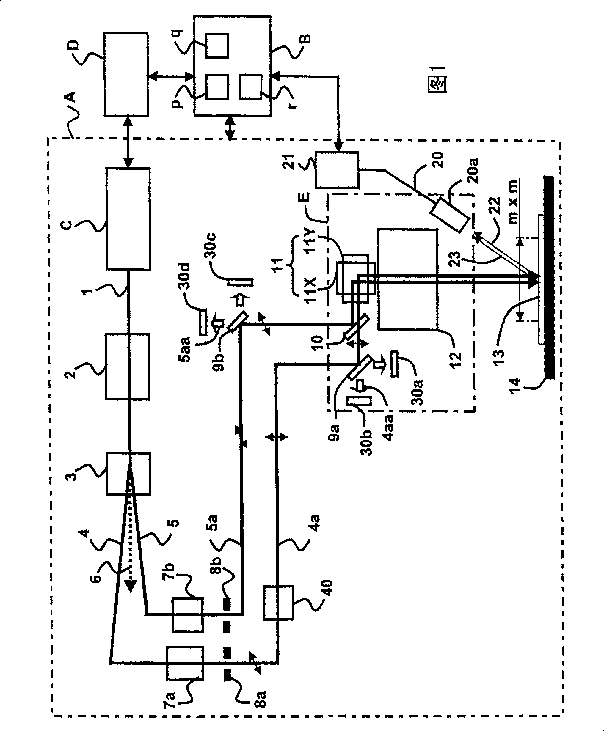
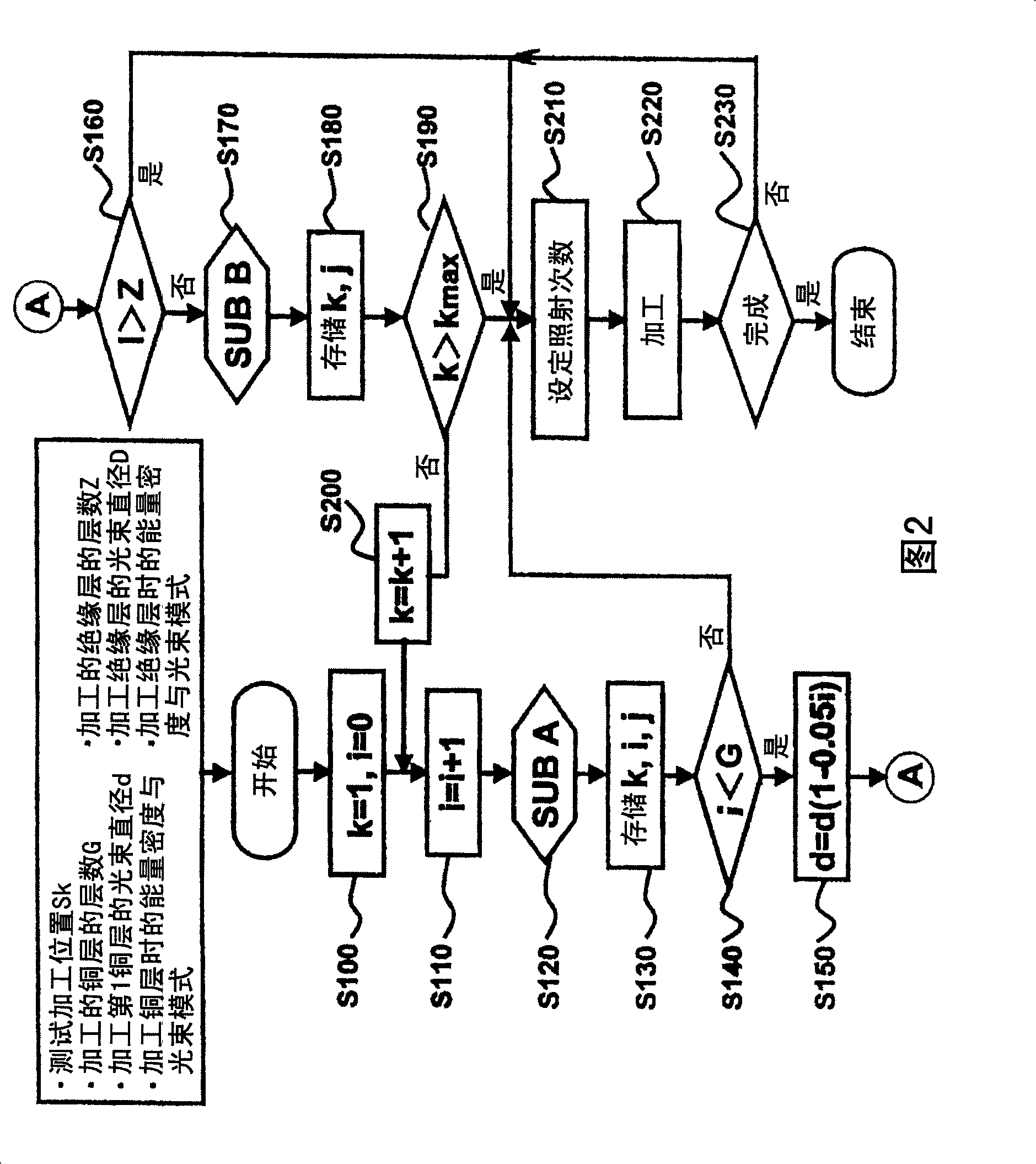
[0044] Fig. 1 is a block diagram of a printed circuit board punching device according to a first embodiment of the present invention.

[0045] The system controller B is connected to the device mechanism unit A, the laser oscillator controller D, and the optical sensor 21 indicated by dotted lines. As will be described later, the system controller B has a comparison unit p that compares the output of the photosensor 21 and photosensors 30a to 30d with a predetermined threshold value, a counter q that counts the number of times the laser beam irradiates the processing part before the comparison unit p operates, and Storage unit r for storing processing conditions and counted number of irradiations.

[0046] The energy density suitable for processing copper and the energy density suitable for processing insulators are prestored in the storage unit r. In addition, in the storage unit r, for each laser mode (energy distribution on a cross section perpendicular to the optical axis...

Embodiment 2

[0122]Here, when the intensity of the reflected light 22 incident on the optical sensor 30b is small, the detection accuracy may decrease.

[0123] Next, a modified example of the present invention will be described.

[0124] Fig. 6 is a front view of the vicinity of a machining head in a modified example (second embodiment) according to the present invention.

[0125] A 1 / 4λ plate 60 is disposed on the printed circuit board 13 side of the condenser lens 12 .

[0126] The 1 / 4λ plate 60 has a characteristic of outputting incident linearly polarized light as circularly polarized light and outputting incident circularly polarized light as linearly polarized light. Also, when the circularly polarized light is reflected by, for example, a mirror, the polarization direction of the reflected circularly polarized light is reversed, that is, the rotation direction changes by 180 degrees. Therefore, when the circularly polarized light whose rotation direction is reversed enters the 1 / ...

Embodiment 3

[0141] 7 is a block diagram showing a schematic configuration of a laser processing apparatus according to a third embodiment of the present invention. In this figure, in the laser processing apparatus according to this embodiment, the processing machine control unit 101 has a positioning control unit 103 for controlling the positioning of a printed circuit board 111 mounted on an X-Y table 112 and a control unit for controlling the irradiation circuit board 111. Laser control section 102 for laser beam 105 . A laser oscillator 104 is connected to the laser control unit 102 , and the laser oscillator 104 emits a laser beam 105 based on an instruction from the laser control unit 102 .

[0142] A mask 106 is disposed below the laser oscillator 104 , and a polarizing beam splitter 107 is disposed further below the mask. The laser beam 105 emitted by the laser oscillator 104 enters the polarized beam splitter 107 through the mask 106 . The polarizing beam splitter 107 is arrange...


PUM

PropertyMeasurementUnit
wavelengthaaaaaaaaaa

Abstract

A method and an apparatus for perforating a printed circuit board are provided so that the processing efficiency and the board densification can be improved. In test processing, a conductor layer 50 i is irradiated with a pulsed laser beam 4 a whose energy density is set at a value high enough to process the conductor layer 50 i while emission 23 a from a processed portion is monitored. Thus, thenumber of pulses of irradiation required for processing a window in the conductor layer 50 i is obtained. An insulating layer 51 i is irradiated with a pulsed laser beam 5 a whose energy density is set at a value high enough to process the insulating layer 51 i but low enough not to process a conductor layer 50 i+1 under the insulating layer 51 i. Thus, the number of pulses of irradiation required for processing a window in the insulating layer 51 i is obtained. The conductor layer 50 i is irradiated with the laser beam 4 a the obtained number of pulses of irradiation, and the insulating layer 51 i is irradiated with the laser beam 5 a the obtained number of pulses of irradiation. Thus, a hole is processed in the printed circuit board.

Description

technical field [0001] The invention relates to a punching method for a printed circuit board and a punching device for a printed circuit board for processing holes on the printed circuit board by pulsed laser beams. Background technique [0002] Now, the pulsed laser beam of UV laser (hereinafter referred to as In the case of punching a hole with a laser beam), when the diameter of the processed hole is 50 μm or more, the diameter is approximately equal to the diameter of the hole entrance, and multiple irradiation energy distributions are required. The cap beam or A Gaussian beam whose energy distribution is a Gaussian curve in the plane direction perpendicular to the optical axis (hereinafter referred to as "punching method"), or a capped beam or Gaussian beam whose diameter is 50 μm or less in diameter smaller than the hole entrance diameter The beam is irradiated while moving, for example, on a circular trajectory, and repeated in the radial direction (hereinafter refe...

Claims


Application Information

Patent Timeline
Patent Type & Authority Patents(China)
IPC IPC(8): H05K3/00B23K26/03
Inventor 荒井邦夫菅原弘之芦泽弘明西山宏美
Owner HITACHI SEIKO LTD
Why Eureka
Try Eureka