Vibration transducer and manufacturing method thereof

A technology of vibration sensors and vibration beams, which is applied in the direction of instruments, microstructure technology, microstructure devices, etc., can solve the problems of devices not working, and achieve the effect of increasing SN ratio, suppressing crosstalk phenomenon, and simple structure

Active Publication Date: 2014-12-17
YOKOGAWA ELECTRIC CORP
View PDF6 Cites 0 Cited by
  • Summary
  • Abstract
  • Description
  • Claims
  • Application Information

AI Technical Summary

Problems solved by technology

This leads to the problem that the vibrating beam sticks to the electrodes, making the device non-functional

Method used


Image

  • Vibration transducer and manufacturing method thereof
  • Vibration transducer and manufacturing method thereof
  • Vibration transducer and manufacturing method thereof

Examples


Embodiment Construction

[0117] Embodiments of the present invention will be described in detail below with reference to the accompanying drawings.

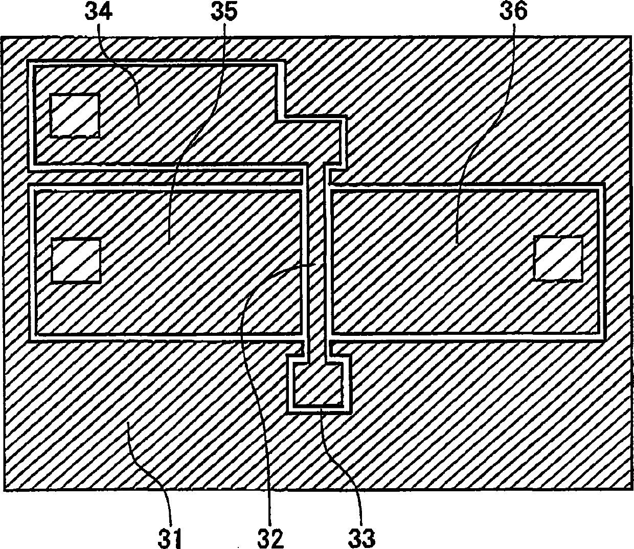
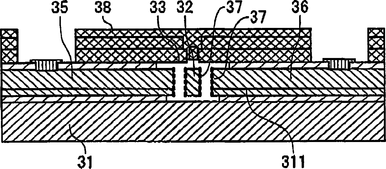
[0118] Figure 1 to Figure 15 Important parts of a vibration sensor according to an embodiment of the present invention are shown. Figure 1A and Figure 1B A plan view and a cross-sectional view showing the configuration of an important part of the vibration sensor assembly, respectively. Figure 2 to Figure 15 The manufacturing process is shown. The following will only describe different Figure 28 components in .

[0119] like Figure 1A and Figure 1B As shown, vibrating beam 32 is arranged in vacuum chamber 33 and tensile stress is exerted on substrate 31 . The vibration beam 32 is single crystal silicon having a cross-sectional shape that is longer in a direction perpendicular to the surface 311 of the substrate 31 than in a direction parallel to the surface 311 .

[0120] The first electrode plate 34 is formed in a plate shape, and is arra...


PUM


Abstract

A vibration transducer includes a silicon single crystal vibration beam provided over a silicon single crystal substrate, the vibration beam having a sectional shape that is longer in a direction perpendicular to a surface of the silicon single crystal substrate than in a direction parallel with it, a shell made of silicon, surrounding the vibration beam with a gap, and forming a vacuum room together with the silicon single crystal substrate, a plate-like first electrode plate disposed parallel with the surface of the silicon single crystal substrate, the first electrode plate having one end connected to the vibration beam, plate-like second and third electrode plates disposed parallel with the surface of the silicon single crystal substrate so as to be opposed to each other with the vibration beam interposed in between, and asperities formed on confronting side surfaces of the vibration beam and the second and third electrode plates.

Description

technical field [0001] The present invention relates to a vibration sensor and a manufacturing method thereof. Background technique [0002] Figures 28 to 37 Important parts of commonly used related art vibration sensors are shown. Figure 28 shows the configuration of the important parts of the vibration sensor assembly, Figure 29 to Figure 37 The manufacturing process is shown. [0003] The manufacturing process will be described below. [0004] First, as Figure 29 As shown, a silicon oxide film 10a is formed on an n-type single crystal silicon substrate 1 and then patterned. [0005] A groove is formed in the substrate 1 by undercutting the removed portion of the oxide film 10a, and is grown in the groove by selective epitaxial growth with 10 18 cm -3 The boron concentration of P + single crystal silicon to form P + Single crystal silicon layer 11 . [0006] Next, in P + The single crystal silicon layer 11 is grown on the surface with 3×10 19 cm -3 or highe...

Claims


Application Information

Patent Timeline
Patent Type & Authority Patents(China)
IPC IPC(8): G01H11/06
CPCB81B2201/0285G01L9/0019B81B2201/0264G01L9/0013B81B2203/0118B81B3/001B81B2201/025G01L1/106H03H9/2457H03H2009/02496
Inventor 吉田隆司
Owner YOKOGAWA ELECTRIC CORP
Why Eureka
Try Eureka