

Sample preparation method and sample preparation equipment for chip failure analysis
A sample preparation and failure analysis technology, which is applied in the field of semiconductors, can solve the problems of low efficiency of failure analysis and time-consuming point needles, etc., and achieve the effect of improving the efficiency of failure analysis
- Summary
- Abstract
- Description
- Claims
- Application Information
AI Technical Summary
Problems solved by technology
Method used
Image

Examples
Embodiment Construction
[0033] The following will clearly and completely describe the technical solutions in the embodiments of the present application with reference to the drawings in the embodiments of the present application. Obviously, the described embodiments are only a part of the embodiments of the present application, not all of them. Based on the embodiments of the present application, all other embodiments obtained by persons of ordinary skill in the art without creative efforts fall within the protection scope of the present application.
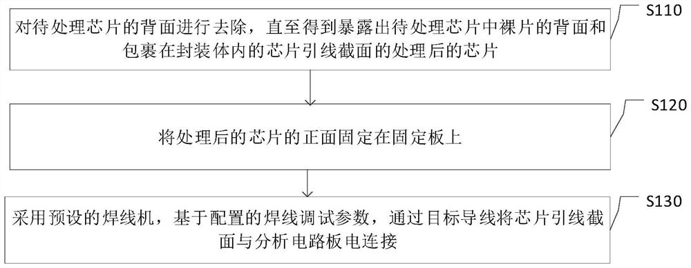
[0034] figure 1 It is a schematic flowchart of a sample preparation method for chip failure analysis provided in the embodiment of the present application. Such as figure 1 As shown, the method may include:
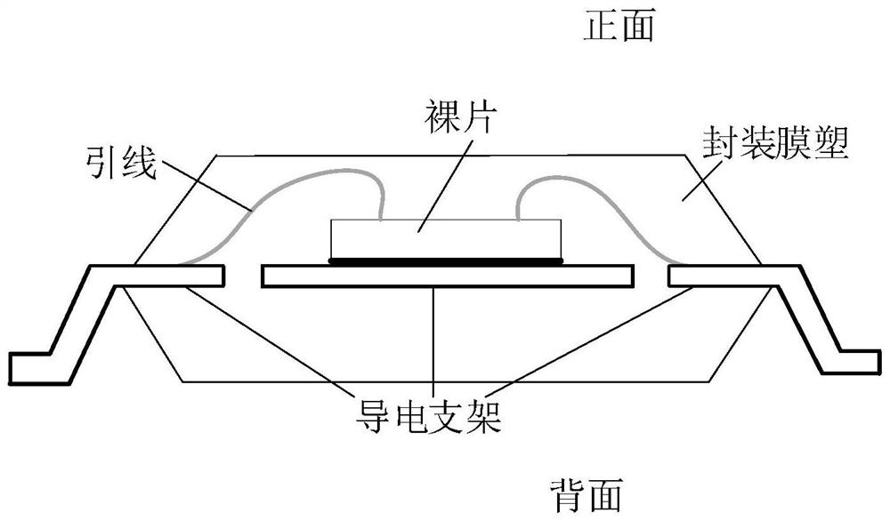
[0035] Step S110 , removing the backside of the chip to be processed until a processed chip is obtained that exposes the backside of the bare chip in the chip to be processed and the section of the lead wire wrapped in the package.
[0036] Suc...
PUM
| Property | Measurement | Unit |
|---|---|---|
| diameter | aaaaa | aaaaa |
| diameter | aaaaa | aaaaa |
Abstract
Description
Claims
Application Information