

Three-dimensional memory and preparation method thereof
A memory and three-dimensional technology, which is applied in semiconductor/solid-state device manufacturing, semiconductor devices, electric solid-state devices, etc., can solve problems such as the complex structure of three-dimensional memory, and achieve the effect of avoiding wafer warping and leakage problems
- Summary
- Abstract
- Description
- Claims
- Application Information
AI Technical Summary
Problems solved by technology
Method used
Image


Examples
Embodiment Construction
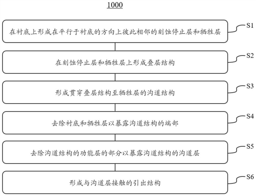
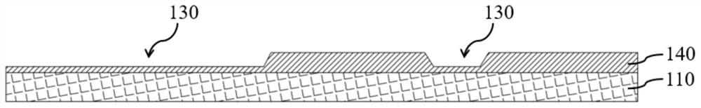
[0029] The present disclosure will be described in detail below in conjunction with the accompanying drawings, and the exemplary embodiments mentioned herein are only used to explain the present disclosure, and are not used to limit the scope of the present disclosure. Throughout the specification, the same reference numerals refer to the same elements.
[0030] In the drawings, the thickness, size and shape of components have been slightly adjusted for convenience of illustration. The drawings are examples only and are not strictly drawn to scale. As used herein, the terms "approximately," "approximately," and similar terms are used to indicate approximations, not degrees, and are intended to describe what would be recognized by one of ordinary skill in the art, measured or calculated inherent bias in .
[0031] It will also be understood that the expression "and / or" includes any and all combinations of one or more of the associated listed items. Expressions such as "compr...
PUM
 Abstract
Description
Claims
Application Information