

Display panel and display device
A technology for display panels and flexible substrates, applied in electrical components, transistors, electrical solid-state devices, etc., can solve problems such as decreased screen display effect, threshold voltage shift, abnormal grayscale display, etc., to achieve normal display and prevent leakage. problems, the effect of improving stability
- Summary
- Abstract
- Description
- Claims
- Application Information
AI Technical Summary
Problems solved by technology
Method used
Image

Examples
Embodiment Construction
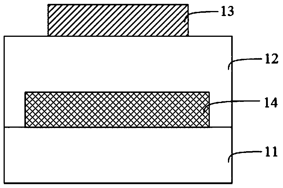
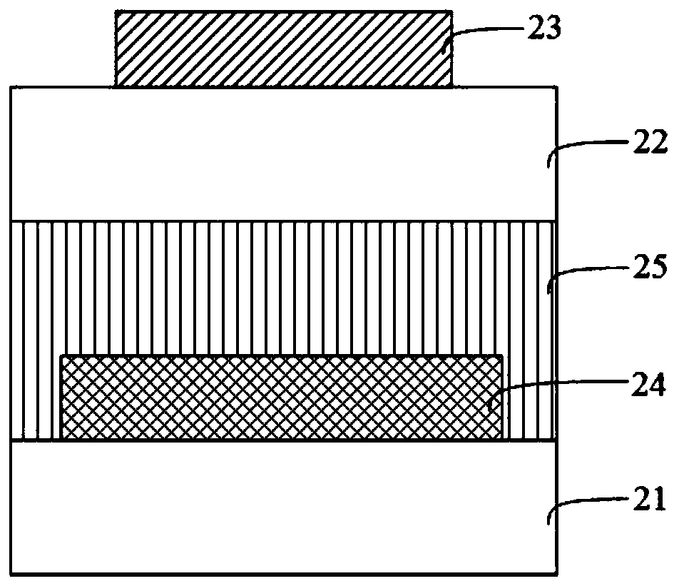
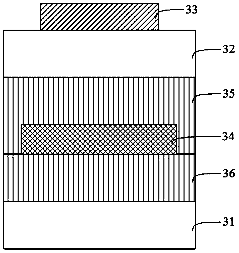
[0022] The analysis found that in the low-temperature polysilicon TFT display panel, the polysilicon active layer is prone to threshold voltage shift when it is irradiated by light, which affects the display effect of the display panel. For example, for a display device with an AMOLED, ambient light and self-luminescence of the display device through multiple emissions (cathode metal layer and source / drain metal layer) will shine on the polysilicon active layer of the transistor, and the polysilicon has The valence band electrons in the source layer and the electrons trapped in the forbidden band defect energy level can easily absorb energy and jump to the conduction band, generating photogenerated electron-hole pairs, which will cause the threshold voltage of the transistor to drift, resulting in abnormal gray scale display and poor image quality. The display effect is reduced.
[0023] To this end, an embodiment of the present invention provides a display panel, including: a...
PUM
 Abstract
Description
Claims
Application Information