
Packaging detection device for semiconductor production

A detection device and semiconductor technology, applied in semiconductor/solid-state device testing/measurement, semiconductor/solid-state device manufacturing, electrical components, etc., can solve problems such as easy wrist fatigue, easy omission, and inconvenient observation, so as to avoid wrist discomfort, Easy to find abnormalities and avoid missed effects

Inactive Publication Date: 2022-04-12
马灿芳
View PDF0 Cites 0 Cited by
  • Summary
  • Abstract
  • Description
  • Claims
  • Application Information

AI Technical Summary

Problems solved by technology

[0002] In the process of semiconductor production, semi-finished semiconductors need to be packaged, and the effect of semiconductor packaging will directly affect whether the semiconductor can work for a long time and with high quality. In mass production of semiconductors, machine vision is often used for automatic and rapid detection, but the detection of machine vision is often planar, and in order to ensure the detection efficiency, it can only be roughly detected, so it is necessary to extract a certain In the traditional detection method, inspectors use a magnifying glass to observe the semiconductor sample from multiple angles, so as to evaluate the packaging effect, and when using a magnifying glass to observe, holding the semiconductor sample to change the angle It is very inconvenient, not only prone to wrist fatigue, but also prone to omissions, and it is easy to change the position of the sample compared to the light source when observing the semiconductor sample, which is easy to make observation inconvenience due to light problems, highlighting its shortcomings

Method used


Image

  • Packaging detection device for semiconductor production
  • Packaging detection device for semiconductor production
  • Packaging detection device for semiconductor production

Examples


Embodiment Construction

[0018] The present invention will be further elaborated below in conjunction with the accompanying drawings and specific embodiments.

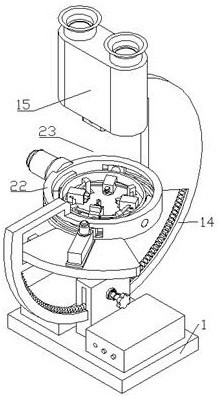
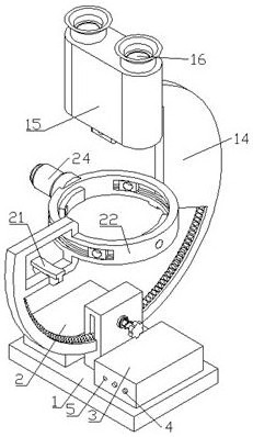
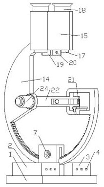
[0019] Such as Figure 1-7 As shown, a packaging and testing device for semiconductor production includes a base 1, a No. 1 battery 2, a No. 2 battery 3, a control button 4, a charging hole 5, a support cylinder 6, a brake ring 7, a radial bearing 8, a gear 9, Adjusting rod 10, brake disc 11, handle 12, No. 1 spring 13, incomplete ring gear frame 14, housing 15, eyepiece 16, objective lens 17, rubber tube 18, lighting lamp 19, adjustment button 20, arc guide rail 21, Support frame 22, swing part 23, described base 1 left part is fixed with No. 1 storage battery 2, and right part is fixed with No. 2 storage battery 3, described No. 1 storage battery 2 and No. Charging hole 5, the control button 4 on the No. 1 storage battery 2 is used to control the inching forward and reverse of the reduction motor 24, and the control button 4 on the No. 2 st...


PUM


Abstract

The invention discloses a packaging detection device for semiconductor production, and the device comprises a pedestal, a first storage battery, a second storage battery, a control button, a charging hole, a supporting cylinder, a brake ring, a radial bearing, a gear, an adjusting rod, a brake disc, a handle, a first spring, an incomplete gear ring frame, a housing, an eyepiece, an objective lens, a rubber cylinder, an illuminating lamp, an adjusting button, an arc-shaped guide rail, a supporting frame, and a swinging part. A first storage battery is fixed to the left portion of the base, a second storage battery is fixed to the right portion of the base, a control button and a charging hole are installed on the front portions of the first storage battery and the second storage battery respectively, a supporting cylinder is rotationally connected to the upper portion of the base, and a brake ring is fixed to the left end of the upper portion of the base. When the brake disc is attached to the brake ring under the action of elastic repulsive force of the second spring, the adjusting rod and the supporting cylinder cannot easily rotate, then the angle stability of the incomplete gear ring frame can be guaranteed, and therefore the stability of the observation process is guaranteed.

Description

technical field [0001] The invention relates to the field of semiconductor production, in particular to a package inspection device for semiconductor production. Background technique [0002] In the process of semiconductor production, semi-finished semiconductors need to be packaged, and the effect of semiconductor packaging will directly affect whether the semiconductor can work for a long time and with high quality. In mass production of semiconductors, machine vision is often used for automatic and rapid detection, but the detection of machine vision is often planar, and in order to ensure the detection efficiency, it can only be roughly detected, so it is necessary to extract a certain In the traditional detection method, inspectors use a magnifying glass to observe the semiconductor sample from multiple angles, so as to evaluate the packaging effect, and when using a magnifying glass to observe, holding the semiconductor sample to change the angle It is very inconveni...

Claims


Application Information

Patent Timeline
Patent Type & Authority Applications(China)
IPC IPC(8): H01L21/67H01L21/66
Inventor 马灿芳
Owner 马灿芳
Learn More