Electromagnetic shielding packaging structure, electronic device module and manufacturing method thereof

A packaging structure, electromagnetic shielding technology, applied in the direction of electrical solid device, semiconductor/solid state device manufacturing, electrical components, etc., can solve the problems of poor electromagnetic shielding effect, difficult high-density integration, etc., to facilitate processing and manufacturing, ensure the shielding effect, The effect of not easily deflected

Active Publication Date: 2022-04-19
CHINA ELECTRONICS TECH GRP NO 26 RES INST
View PDF5 Cites 0 Cited by
  • Summary
  • Abstract
  • Description
  • Claims
  • Application Information

AI Technical Summary

Problems solved by technology

[0003] In view of the shortcomings of the prior art described above, the purpose of the present invention is to provide an electromagnetic shielding packaging structure, an electronic device module and a manufacturing method thereof, which are used to solve the problem of poor electromagnetic shielding effect between compartments in the prior art and difficulty in high-density integration problem

Method used


Image

  • Electromagnetic shielding packaging structure, electronic device module and manufacturing method thereof
  • Electromagnetic shielding packaging structure, electronic device module and manufacturing method thereof
  • Electromagnetic shielding packaging structure, electronic device module and manufacturing method thereof

Examples


Embodiment Construction

[0030] Embodiments of the present invention are described below through specific examples, and those skilled in the art can easily understand other advantages and effects of the present invention from the content disclosed in this specification. The present invention can also be implemented or applied through other different specific implementation modes, and various modifications or changes can be made to the details in this specification based on different viewpoints and applications without departing from the spirit of the present invention.

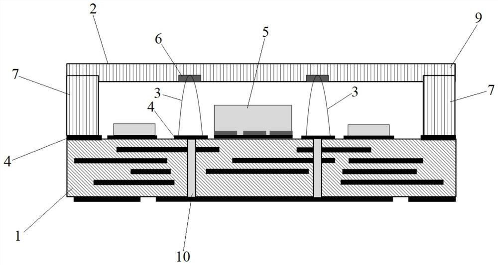
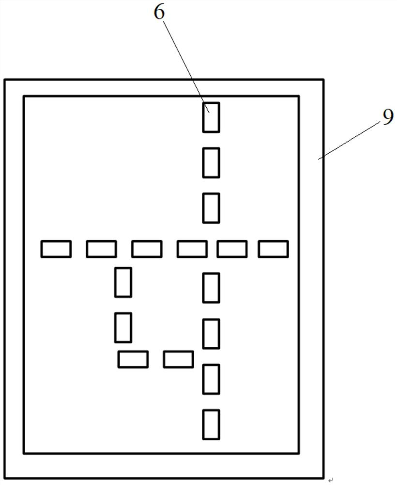
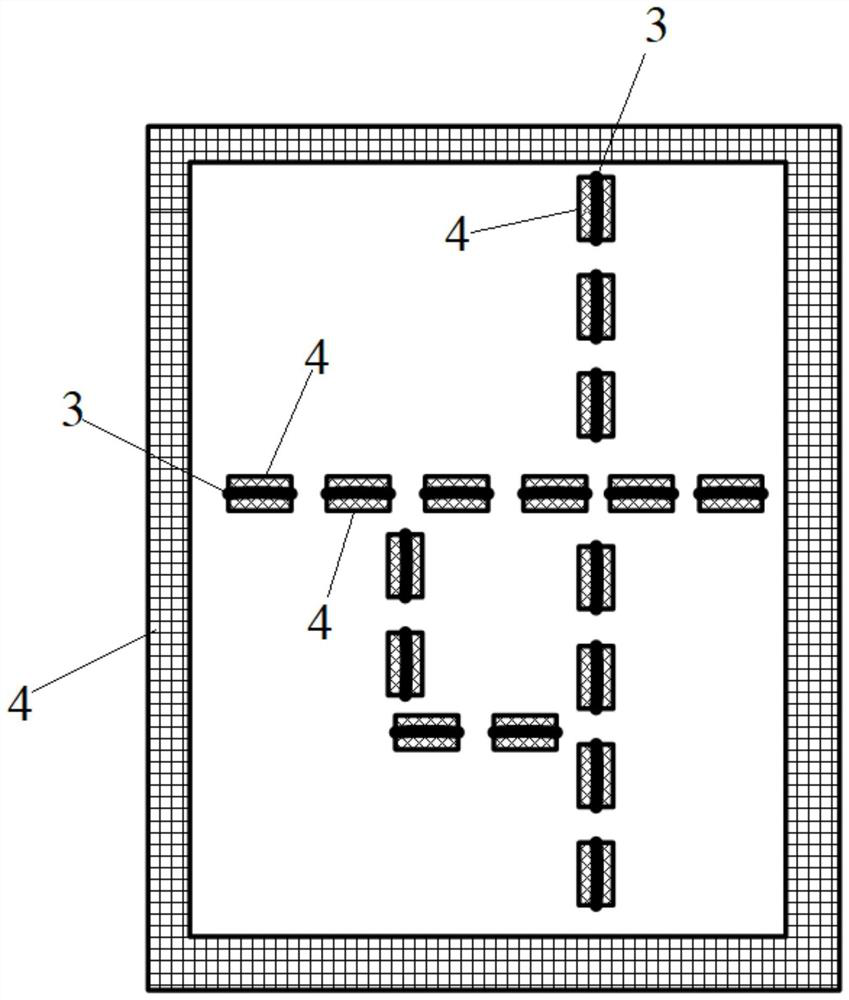
[0031] It should be noted that the diagrams provided in this embodiment are only schematically illustrating the basic idea of ​​the present invention, and only the components related to the present invention are shown in the diagrams rather than the number, shape and shape of the components in actual implementation. Dimensional drawing, the type, quantity and proportion of each component can be changed arbitrarily during actual impleme...


PUM


Abstract

The invention provides an electromagnetic shielding packaging structure, an electronic device module and a manufacturing method thereof, and belongs to the technical field of semiconductor electronic device modules. The electromagnetic shielding packaging structure comprises a first shielding piece, a second shielding piece and a lead, the two ends of the lead are conductively connected to the first shielding piece respectively, a connecting part is arranged between the two ends of the lead, and the connecting part is bent and conductively connected to the second shielding piece; the electronic device module comprises the electromagnetic shielding packaging structure and further comprises an electronic component, and the electronic component is arranged between the first shielding piece and the second shielding piece. The manufacturing method of the electronic device module comprises the following steps that the two ends of the lead are conductively connected to the first shielding piece, the connecting part is bent in the direction away from the first shielding piece, and the connecting part is conductively connected to the second shielding piece. The shielding effect is good, high-density integration of multiple electronic devices is facilitated, the lead strength is improved, deflection and toppling are not prone to occurring, and machining and manufacturing are convenient.

Description

technical field [0001] The invention relates to semiconductor electronic device module technology, in particular to an electromagnetic shielding packaging structure, an electronic device module and a manufacturing method thereof. Background technique [0002] At present, a metal frame and a cover are usually installed on the circuit board to realize electromagnetic shielding of the internal circuit of the radio frequency module. The electronic components inside the module are isolated by the shielding partition wall set inside the metal frame. In the existing process, the metal frame and the cover are welded together by parallel seam welding. The cover can only be connected around the outer frame of the metal frame, but the top of the shielding partition inside the metal frame and the cover cannot be welded. , It is prone to poor contact connection and poor conduction, resulting in poor electromagnetic shielding effect between compartments. In addition, the thickness of th...

Claims


Application Information

Patent Timeline
Patent Type & Authority Applications(China)
IPC IPC(8): H01L23/552H01L21/50H01L21/52
CPCH01L23/552H01L21/50H01L21/52
Inventor 余怀强
Owner CHINA ELECTRONICS TECH GRP NO 26 RES INST
Why Eureka
Try Eureka