Supercharge Your Innovation With Domain-Expert AI Agents!

Low-power-consumption large-slew-rate low-distortion output stage circuit

An output stage circuit, high slew rate technology, applied in the direction of improving amplifiers to reduce nonlinear distortion, negative feedback circuit layout, etc., to achieve the effects of low quiescent current, low power consumption, and large slew rate

Pending Publication Date: 2022-04-22
GUIZHOU ZHENHUA FENGGUANG SEMICON
View PDF0 Cites 0 Cited by
  • Summary
  • Abstract
  • Description
  • Claims
  • Application Information

AI Technical Summary

Problems solved by technology

[0018] The purpose of the invention is to: solve the following three major problems in the existing Class A and B output stage circuits:

Method used


Image

  • Low-power-consumption large-slew-rate low-distortion output stage circuit
  • Low-power-consumption large-slew-rate low-distortion output stage circuit
  • Low-power-consumption large-slew-rate low-distortion output stage circuit

Examples


Embodiment Construction

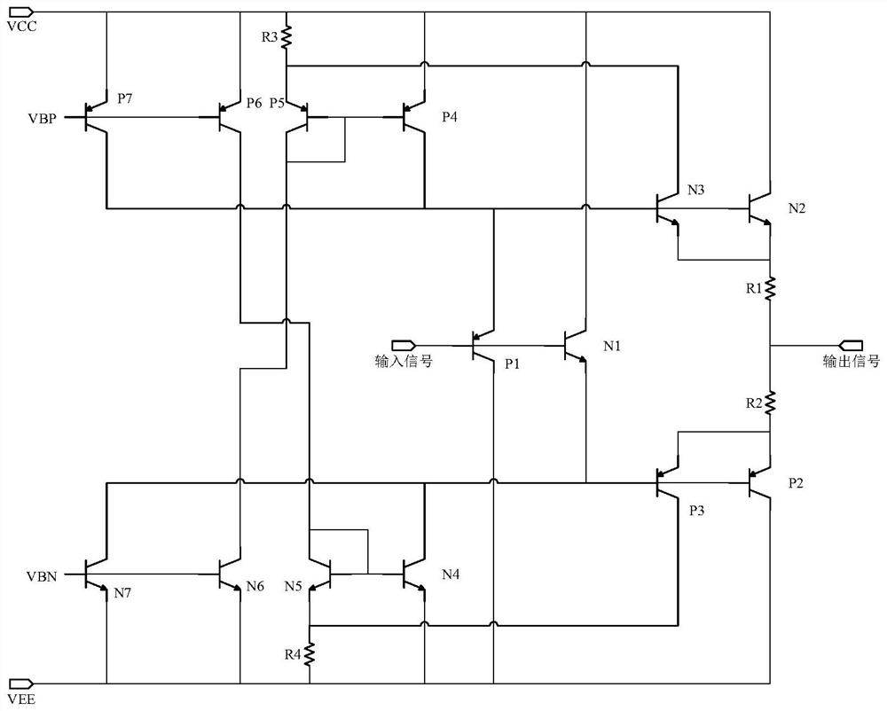
[0103] Such as Figure 5 Shown, embodiment of the present invention is as follows:

[0104] In the layout of the integrated circuit, the input units P1, N1, and the output units P2, N2, R1, R2 are divided into several equal groups, and each group is correspondingly connected.

[0105] N3 and P3 respectively sample the current of one of N2 and P2, and the sampled current is sent to R3 and R4 respectively to increase the current of P4 and N4 when outputting a large current.

[0106] Taking the base of P4 as the disconnection point of the AC loop, the loop gain is

[0107] GH=g mP4 beta N2 K N3N2 R3

[0108] Taking the base of N4 as the disconnection point of the AC loop, the loop gain is

[0109] GL=g mN4 beta P2 K P3P2 R4

[0110] where g mP4 is the transconductance of P4, g mN4 is the transconductance of N4, β N2 is the current gain of N2 in the case of high current, β P2 It is the current gain of P2 in the case of high current. By parameter adjustment, both GH ...


PUM


Abstract

The invention discloses a low-power-consumption large-slew-rate low-distortion output stage circuit, and belongs to the field of integrated circuits. Comprising an emitter follower, a bias current source, a class AB output stage circuit, a driving tube bias current positive feedback circuit, a capacitance coupling circuit and a collector voltage synchronous tracking circuit. The driving tube bias current positive feedback circuit carries out sampling and positive feedback on output stage current, the capacitance coupling circuit is located between base electrodes of an output device, and the collector voltage synchronous tracking circuit connects a collector electrode of an emitter follower with an emitter electrode of a class AB output stage circuit. And the collector voltage of the emitter follower and the emitter voltage of the class AB output stage circuit change synchronously. The problems that an existing class AB output stage circuit is low in power consumption, low in slew rate and large in distortion are solved. The purposes of low quiescent current, high slew rate and low distortion are achieved through the technical schemes of driving tube bias current positive feedback, capacitance coupling, collector voltage synchronous tracking and the like. The circuit is widely applied to low-power-consumption, large-slew-rate and low-distortion output stage circuits.

Description

technical field [0001] The invention belongs to the field of integrated circuits, and further relates to a low power consumption, large slew rate and low distortion output stage circuit. Background technique [0002] In transistor amplifiers, Class A and B output stage circuits are widely used for their low quiescent current and small crossover distortion. Quiescent current, slew rate and distortion are important specifications for Class A and B output stage circuits. [0003] Such as figure 1 Shown is a traditional Class A and B output stage circuit structure. The PNP device P1 and the NPN device N1 constitute emitter followers, respectively. And current source I1 provides bias current for P1, and current source I2 provides bias current for N1. NPN device N2 and PNP device P2 are output devices, which can provide large current for the load. R1 and R2 are emitter degeneration resistors, which are used to make the current of N2 and P2 more uniform and avoid current conce...

Claims


Application Information

Patent Timeline
IPC IPC(8): H03F1/32H03F1/34
CPCH03F1/32H03F1/34
Inventor 周文质包磊唐拓李政陈旺云田瑾民王平霜王志超
Owner GUIZHOU ZHENHUA FENGGUANG SEMICON
Features
  • R&D
  • Intellectual Property
  • Life Sciences
  • Materials
  • Tech Scout
  • Unparalleled Data Quality
  • Higher Quality Content
  • 60% Fewer Hallucinations
Learn More