Multi-channel bandwidth signal generation device and method with wide frequency band coverage
A signal generation device and frequency band coverage technology, applied in the directions of radio transmission systems, electrical components, transmission systems, etc. Large and other problems, to achieve the effect of rich external interfaces, wide frequency coverage, and high interface speed
- Summary
- Abstract
- Description
- Claims
- Application Information
AI Technical Summary
Problems solved by technology
Method used
Image
Examples
Embodiment 1
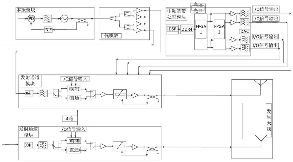
[0033] Such as figure 1 As shown, the present invention is a multi-channel bandwidth signal generating device with wide frequency band coverage, including a signal generating channel and an intermediate frequency baseband processing module.
[0034] Signal generating channel, including generating antenna, low noise amplifier module, transmitting channel module and local oscillator module;
[0035] An antenna configured for wireless signal transmission and frequency band coverage expansion;
[0036] A low-noise amplification module configured to amplify signals;
[0037] a transmitting channel module configured for signal modulation and signal transmission;
[0038] The local oscillator module is configured to configure signal frequency points;
[0039] IF baseband processing module, including multiple DAC, FPGA, DSP and DDR4;
[0040] a DAC configured for sampling transmission of the signal;
[0041] FPGA, including FPGA1 and FPGA2; configured for system control and data ...
Embodiment 2
[0052] On the basis of the above-mentioned embodiment 1, the present invention also mentions a method for generating a wide-bandwidth signal with multi-channel frequency band coverage, which specifically includes the following steps:
[0053] Step 1: DSP receives the main control data through the network port, combines and subpackages the main control data, and sends the data to FPGA1 through identification and marking;
[0054] Step 2: FPGA1 receives data through its SRIO port, stores the received data in DDR4, and transmits the stored data to FPGA2 through the high-speed optical port;
[0055] Step 3: FPGA2 performs interpolation processing on the received data, and then sends it to DAC;
[0056] Step 4: DAC sends the sent data to the transmit channel module according to the configured sampling rate and channel mode;
[0057] Step 5: Transmit the channel module, modulate the data to the corresponding frequency point, and control the power of the signal;
[0058] Step 6: Th...
Embodiment 3
[0060] On the basis of the foregoing embodiments, the present invention provides a baseband processing method, comprising the following steps:
[0061] Step S1: Multi-map the IQ data of the baseband signal to be generated, transmit it through the SRIO port, and then write DDR4 in FPGA1;
[0062] Step S2: Use a ping-pong structure when writing DDR4. When storing data, the rate of data to be generated is basically the rate of the SRIO port, and the writing rate of DDR can meet;
[0063]Step S3: In order to meet the write burst length design of DDR4 when writing DDR4, connect FIFO (First Input First Output, that is, the first-in-first-out queue), and at least meet the minimum amount of data in the design to start writing to DDR4;
[0064] Step S4: When reading DDR4, in order to avoid signal loss caused by too fast read rate, connect FIFO, and stop reading data from DDR when it is recognized that FIFO is almost full, so as to achieve continuous data reading;
[0065] Step S5: Aft...
PUM
 Abstract
Description
Claims
Application Information
