Planar power MOSFET device integrated with junction barrier Schottky diode

A junction barrier Schottky and diode technology, applied in semiconductor devices, electrical components, circuits, etc., can solve problems such as partial conflict in the active area

Pending Publication Date: 2022-04-26
海科(嘉兴)电力科技有限公司
View PDF0 Cites 1 Cited by
  • Summary
  • Abstract
  • Description
  • Claims
  • Application Information

AI Technical Summary

Problems solved by technology

[0005] The embodiment of the present application provides a planar power MOSFET device with an integrated junction barrier Schottky diode, which is used to solve the problem that the existing junction barrier Schottky cells and MOSFET cells occupy the active region of the device together. There are conflicting technical issues
[0007] The planar power MOSFET device with integrated junction barrier Schottky diode provided by the embodiment of the present application not only solves the existing junction barrier Schottky cell and MOSFET cell fusion through the special design The special base cell and the MOSFET cell have the problem of conflict when they jointly occupy the active area of ​​the device, and it also ensures that the junction barrier Schottky diode has a relatively high performance under the premise of small MOSFET device conduction loss. High current conduction capability

Method used


Image

  • Planar power MOSFET device integrated with junction barrier Schottky diode
  • Planar power MOSFET device integrated with junction barrier Schottky diode
  • Planar power MOSFET device integrated with junction barrier Schottky diode

Examples


Embodiment Construction

[0027] In order to make the purpose of the present application, the technical solution and advantages more clear, the following will be combined with the specific embodiments of the present application and the corresponding drawings of the technical solution of the application is clearly and completely described. Obviously, the embodiments described are only a portion of the present application, not all embodiments. Based on the embodiments in the present application, all other embodiments obtained by those of ordinary skill in the art without doing creative labor, are within the scope of protection of the present application.

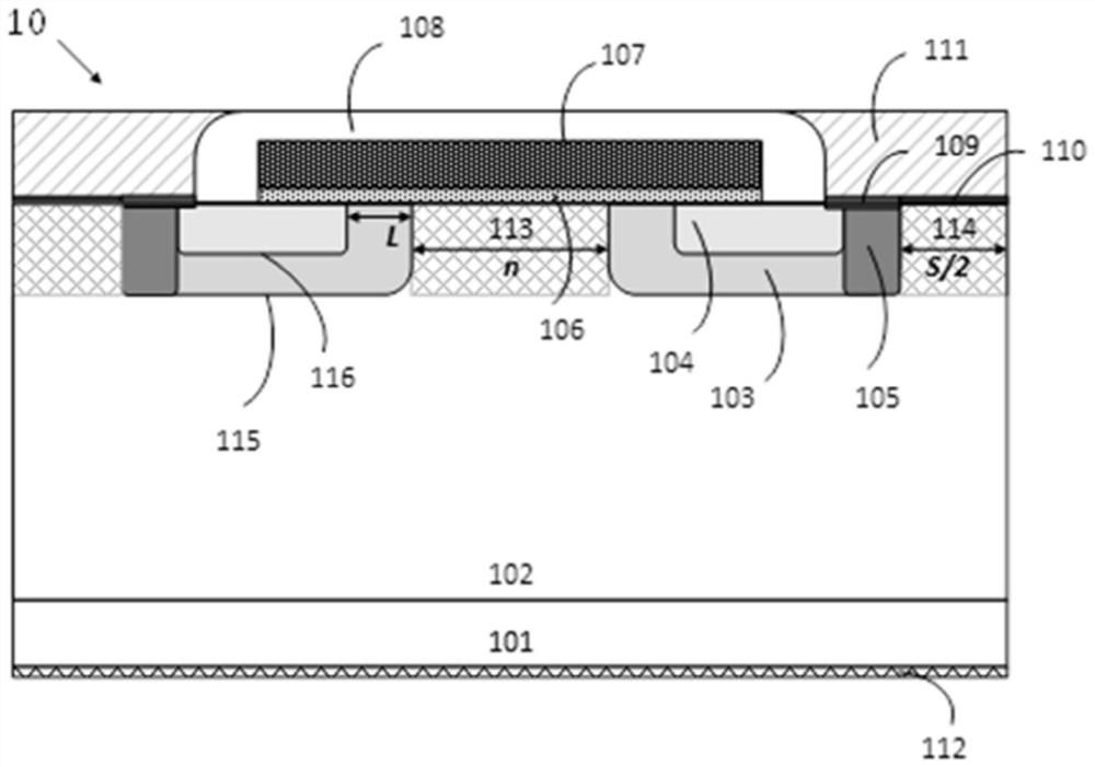
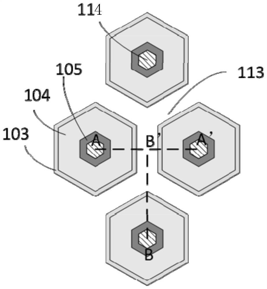
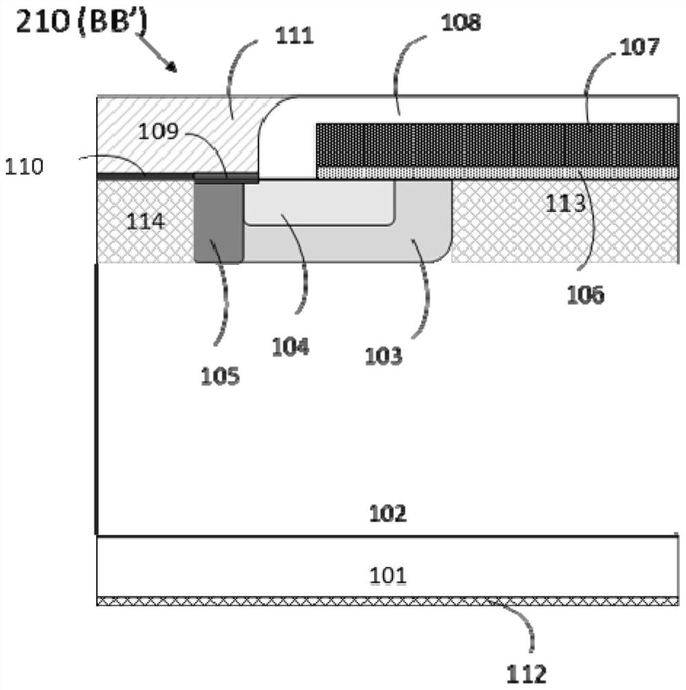
[0028] Embodiment of the present application provides a planar power MOSFET device integrating a junction barrier Schottky diode to solve the existing junction barrier Schottky cells and MOSFET cells, there are conflicting technical problems when jointly occupying the active region portion of the device.

[0029] The following technical solution proposed b...


PUM


Abstract

The invention discloses a planar power MOSFET (Metal-Oxide-Semiconductor Field Effect Transistor) device integrated with a junction barrier Schottky diode, which is used for solving the technical problem that conflicts exist when existing junction barrier Schottky cells and MOSFET cells jointly occupy an active region part of the device. The device comprises an epitaxial layer; a plurality of cells with the same shape and structure are distributed on the first side surface of the epitaxial layer; each cell at least comprises a well region, a source region, a highly doped P-type region and a Schottky region; the well region is in contact with the highly-doped P-type region, and the highly-doped P-type region surrounds the Schottky region; junction field effect transistor (JFET) regions are formed between adjacent well regions. A first PN junction is formed between the well region and the epitaxial layer; a second PN junction is formed between the well region and the source region; the value range of the width of the JFET region and the value range of the spacing of the highly doped P-type region are in the same preset interval. Through the device, the problem that conflicts exist when junction barrier Schottky cells and MOSFET cells jointly occupy the active region part of the device is solved.

Description

Technical field [0001] The present application relates to the field of semiconductor manufacturing technology, in particular to the integrated junction Schottky diode planar power MOSFET device. Background [0002] There is a base plane dislocation (BPD) in a silicon carbide crystal, and under certain conditions, the base plane dislocation (BPD) can be converted into a stacking layer fault (SF). When the bulk diode in the SiC power MOSFET device is turned on, the electron-hole composite will continue to expand the stack layer fault (SF) under bipolar operation, and bipolar degradation will occur. This phenomenon increases the on-voltage resistance of the silicon carbide power MOSFET, the leakage current in the blocking mode increases, and the on-voltage drop of the body diode increases, thereby reducing the reliability of the device. [0003] In practical circuit applications, to avoid bipolar degradation, designers typically use external reverse parallel Schottky diodes to supp...

Claims


Application Information

Patent Timeline
Patent Type & Authority Applications(China)
IPC IPC(8): H01L29/78H01L29/06
CPCH01L29/7804H01L29/0615
Inventor 于霄恬
Owner 海科(嘉兴)电力科技有限公司
Why Eureka
Try Eureka