Memory, reading operation method thereof and memory system
A read operation, memory technology, applied in the semiconductor field, can solve problems such as read operation failure
- Summary
- Abstract
- Description
- Claims
- Application Information
AI Technical Summary
Problems solved by technology
Method used
Image
Examples
Embodiment Construction
[0053] In order to make the technical solutions and advantages of the embodiments of the present invention more clear, the specific technical solutions of the invention will be further described in detail below in conjunction with the drawings in the embodiments of the present invention.
[0054] The memory in the embodiment of the present invention includes but is not limited to a 3D NAND memory, and for ease of understanding, a 3D NAND memory is used as an example for illustration.
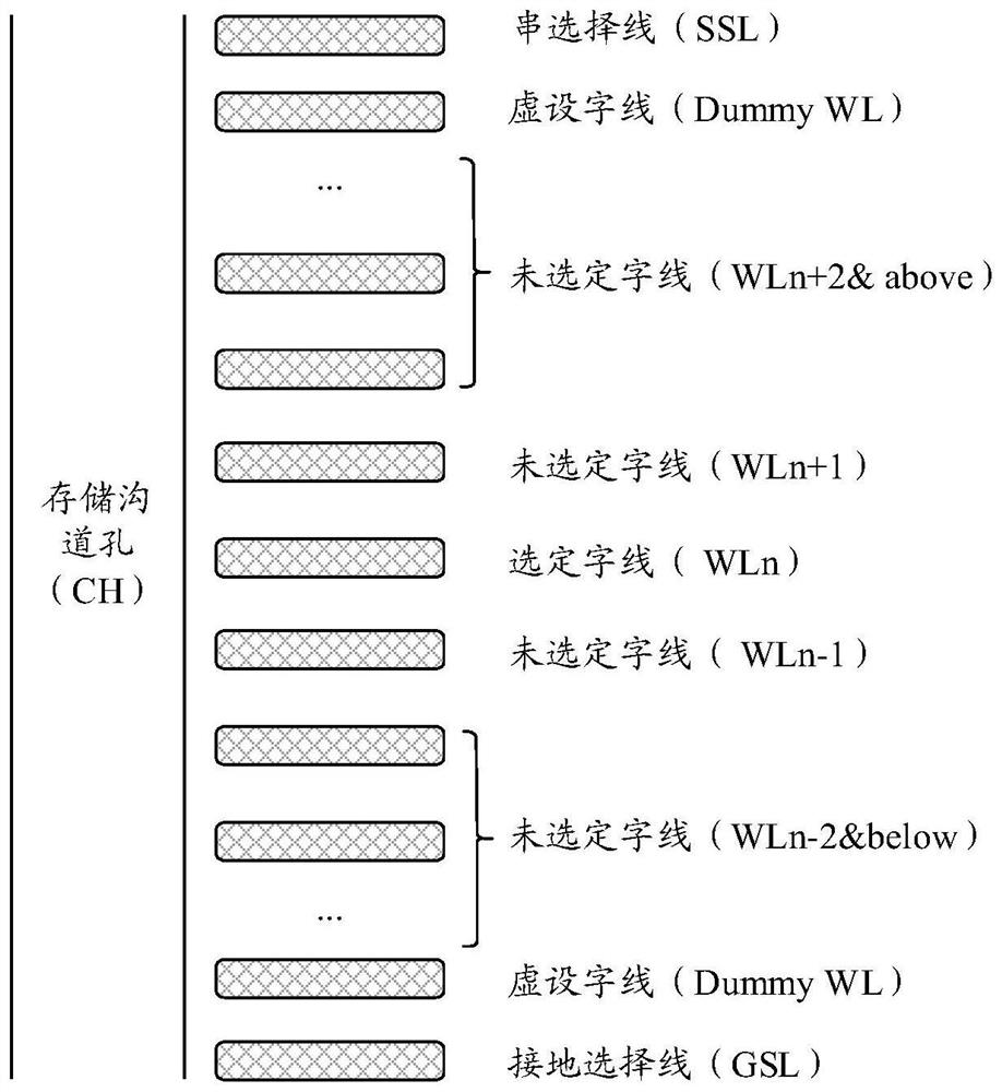
[0055] In practical applications, the 3D NAND memory may include a memory cell array and peripheral circuits; wherein, the memory cell array may include a plurality of memory strings; each memory string may include a plurality of memory cells stacked in a vertical direction . Each memory cell can be programmed and store one or more bits of data.
[0056] Specifically, the memory cell array of the 3D NAND type memory may specifically include: a semiconductor substrate: a plurality of gate layers a...
PUM
 Abstract
Description
Claims
Application Information


