Supercharge Your Innovation With Domain-Expert AI Agents!

Chip packaging structure

A chip packaging structure, chip technology, applied in the direction of electrical components, electrical solid devices, circuits, etc., can solve the problems of reliability risk, vertical size increase, etc., to save bonding gold wire, reduce the vertical size, avoid chip displacement bit effect

Pending Publication Date: 2022-04-29
NANTONG FUJITSU MICROELECTRONICS
View PDF0 Cites 0 Cited by
  • Summary
  • Abstract
  • Description
  • Claims
  • Application Information

AI Technical Summary

Problems solved by technology

Gasket stacking and FOW methods require two bonding wires to be bonded on the same BondFinger, which requires a larger Bond Finger to be designed on the substrate, which cannot be satisfied by the existing substrate size.
At the same time, these two solutions will increase the longitudinal dimension of the entire package, and the two bonding wires on the same Bond Finger will also bring reliability risks

Method used


Image

  • Chip packaging structure
  • Chip packaging structure
  • Chip packaging structure

Examples


Embodiment Construction

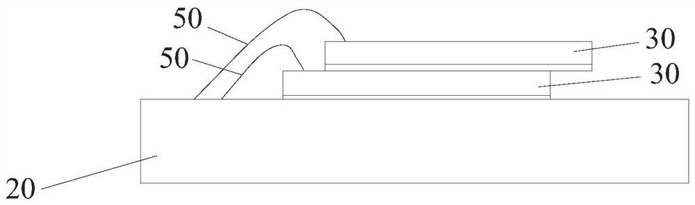
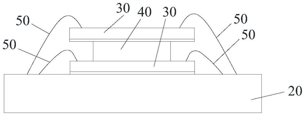
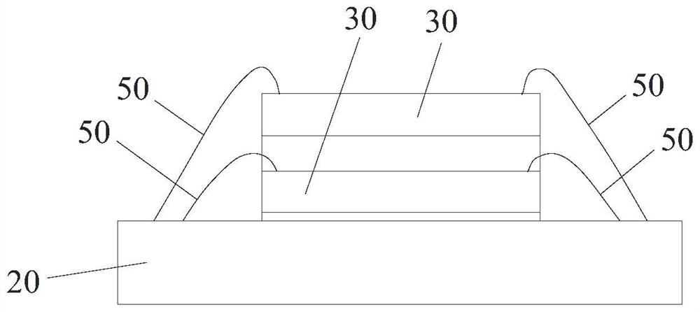
[0052] The following will clearly and completely describe the technical solutions in the embodiments of the present application with reference to the accompanying drawings in the embodiments of the present application. Obviously, the described embodiments are only part of the embodiments of the present application, not all of them. Based on the embodiments in this application, all other embodiments obtained by persons of ordinary skill in the art without making creative efforts belong to the scope of protection of this application.

[0053] It should be noted that when an element is referred to as being “disposed on” another element, it may be directly on the other element or there may be another element in between. When an element is referred to as being "connected to" another element, it can be directly connected to the other element or it may be present intervening with the other element. The terms "vertical," "horizontal," "left," "right," and similar expressions are used ...


PUM


Abstract

The invention discloses a chip packaging structure. The chip packaging structure comprises a substrate; the first chip layer is located on one side of the substrate and comprises one or more chips, and the non-functional surfaces of the chips of the first chip layer face the substrate; the first rewiring layer is positioned on one side, back to the substrate, of the first chip layer and is electrically connected with a functional surface of a chip of the first chip layer; the second chip layer is located on the side, back to the first chip layer, of the first rewiring layer and comprises one or more chips, and the functional faces of the chips of the second chip layer face the first rewiring layer and are electrically connected with the first rewiring layer; the second re-wiring layer is positioned on one side, back to the first re-wiring layer, of the second chip layer and is electrically connected with the first re-wiring layer; one end of the bonding wire is electrically connected with the second rewiring layer, and the other end of the bonding wire is electrically connected with the substrate. According to the chip packaging structure provided by the invention, longitudinal and vertical stacking of three-dimensional multiple chips can be realized, the transverse space of the substrate is saved, and the cost is saved.

Description

technical field [0001] The present application relates to the technical field of semiconductors, in particular to a chip packaging structure. Background technique [0002] The descriptions in this section only provide background information related to the disclosure in this specification and may not constitute prior art. [0003] In the packaging industry, the structure in which devices are arranged horizontally in the system-in-package is the simplest and the easiest to obtain high yield, so it is the most widely used. However, as the demand for miniaturization of packages increases, in order to further reduce the volume, chips or devices need to be stacked in the vertical direction. [0004] The 3D package is realized by stacking chips, and the interconnection after stacking can usually be realized by wire bonding or through silicon via (Through Silicon Via, TSV). TSV technology has relatively large limitations and high cost, while wire bonding is a relatively traditiona...

Claims


Application Information

Patent Timeline
Patent Type & Authority Applications(China)
IPC IPC(8): H01L23/498H01L23/538
CPCH01L23/49811H01L23/49838H01L23/5386H01L2224/8592H01L2224/05H01L2224/18H01L2224/73265H01L2224/32145
Inventor 沈鹏飞
Owner NANTONG FUJITSU MICROELECTRONICS
Features
  • R&D
  • Intellectual Property
  • Life Sciences
  • Materials
  • Tech Scout
  • Unparalleled Data Quality
  • Higher Quality Content
  • 60% Fewer Hallucinations
Learn More