Wafer double-power cutting method and optical path device

A cutting method and dual-power technology, which is applied in laser welding equipment, metal processing equipment, welding equipment, etc., can solve the problems of inapplicable hidden cutting method and inability to adjust laser power

Inactive Publication Date: 2022-05-03
深圳市圭华智能科技有限公司
View PDF0 Cites 0 Cited by
  • Summary
  • Abstract
  • Description
  • Claims
  • Application Information

AI Technical Summary

Problems solved by technology

[0004] The object of the present invention is to provide a dual-power wafer cutting method and an optical path device to solve the above-mentioned background

Method used


Image

  • Wafer double-power cutting method and optical path device
  • Wafer double-power cutting method and optical path device
  • Wafer double-power cutting method and optical path device

Examples


Embodiment Construction

[0026] The following will clearly and completely describe the technical solutions in the embodiments of the present invention with reference to the accompanying drawings in the embodiments of the present invention. Obviously, the described embodiments are only some, not all, embodiments of the present invention. Based on the embodiments of the present invention, all other embodiments obtained by persons of ordinary skill in the art without making creative efforts belong to the protection scope of the present invention.

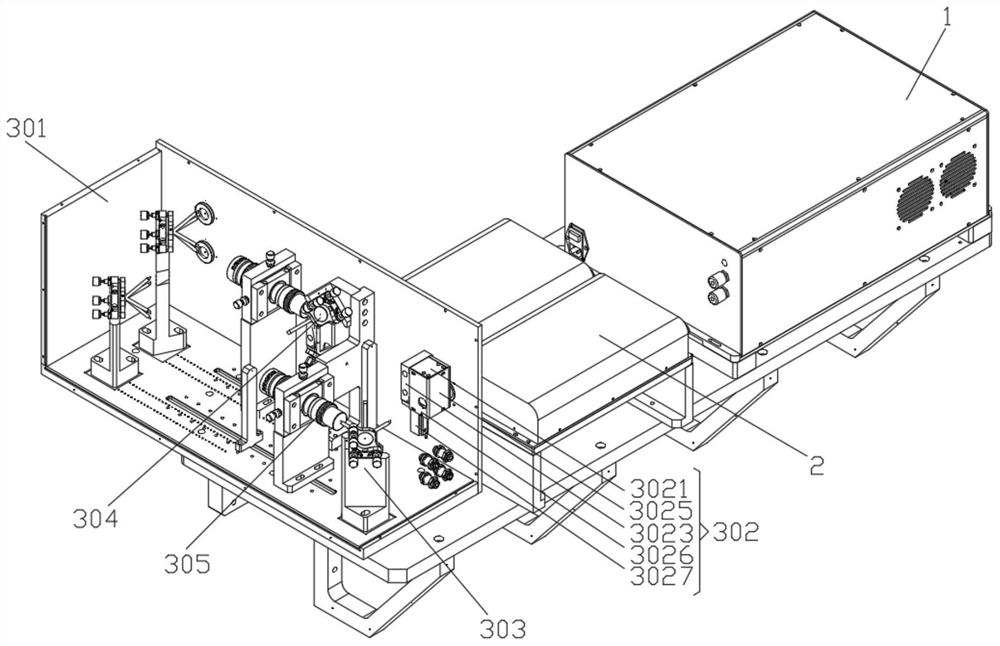
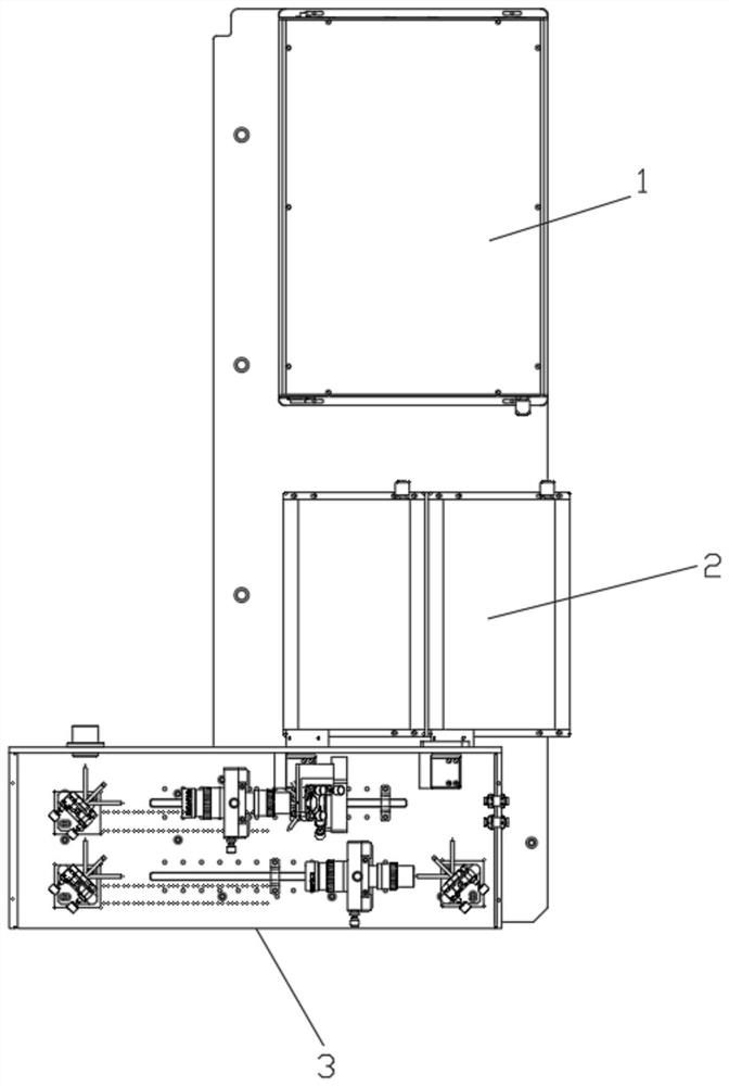
[0027] see Figure 1-6 , the present invention provides a technical solution: a wafer dual power cutting method, the steps are as follows:

[0028] Step 1, emit laser A through dual-port laser 1;

[0029] Step 2. Laser A converts laser A into laser B and laser C with different powers through two different laser power converters 2;

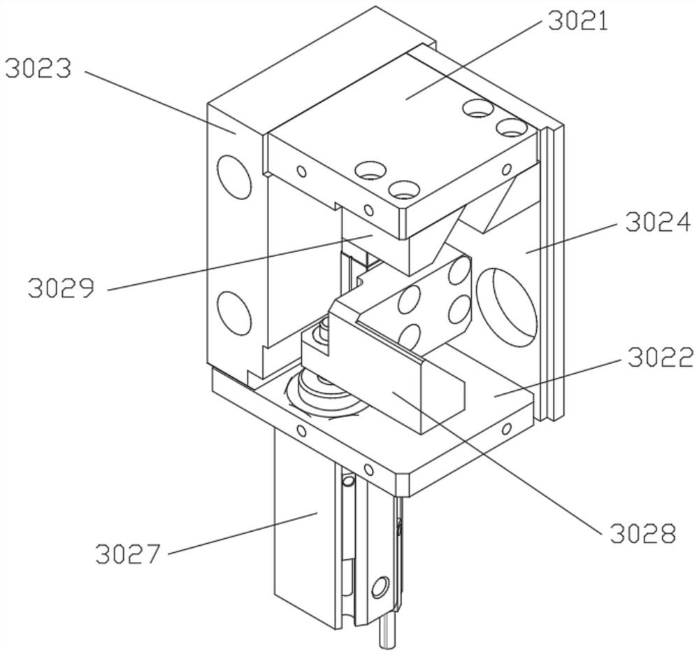
[0030] Step 3. Laser B and laser C pass through two shutter devices 302 respectively, and the two shutter devices 302 are used ...


PUM


Abstract

The invention discloses a wafer double-power cutting method. The method comprises the steps that 1, laser A is emitted through a double-port laser; 2, the laser A passes through two different laser power converters, and the laser A is converted into laser B and laser C which are different in power; step 3, the laser B and the laser C respectively pass through two optical gate devices, and the two optical gate devices are both used for releasing and closing the laser; 4, the laser B and the laser C are subjected to beam expanding through two beam expanding devices; step 5, turning the laser B and the laser C after beam expansion through a turning optical cavity assembly; step 6, converging the steered laser B and laser C together through a light path converging light cavity assembly; 7, the converged laser B and laser C are emitted at the same position through a light emitting cavity assembly; according to the invention, after the laser is split, the opening and closing of the two light paths are regulated and controlled, the emergent light with different powers can be provided as required, and the implicit cutting requirements of wafers are met.

Description

technical field [0001] The invention relates to the technical field of wafer cutting, and specifically relates to a wafer dual-power cutting method and an optical path device. Background technique [0002] Wafer refers to the silicon wafer used in the production of silicon semiconductor integrated circuits. Because of its circular shape, it is called a wafer; it can be processed into various circuit element structures on the silicon wafer, and become an IC with specific electrical functions. product. [0003] At present, in the process of wafer processing, the laser power used cannot be adjusted, so it is not suitable for implicit cutting. Contents of the invention [0004] The object of the present invention is to provide a dual-power wafer cutting method and an optical path device to solve the above-mentioned background technology. At present, in the process of wafer processing, the laser power used cannot be adjusted, so it is not suitable for implicit cutting. The pr...

Claims


Application Information

Patent Timeline
IPC IPC(8): B23K26/064B23K26/38
CPCB23K26/064B23K26/38
Inventor 叶宗辉周建红
Owner 深圳市圭华智能科技有限公司
Why Eureka
Try Eureka