Nonlinear semiconductor light sources

a semiconductor and light source technology, applied in semiconductor lasers, optical resonator shape and construction, instruments, etc., can solve the problems of insufficient optics, complex conventional sources of parametric and/or harmonic light, and inability to achieve geometric optimal coupling configurations,

Inactive Publication Date: 2004-11-09
ALCATEL-LUCENT USA INC +1
View PDF4 Cites 78 Cited by
  • Summary
  • Abstract
  • Description
  • Claims
  • Application Information

AI Technical Summary

Problems solved by technology

Such conventional sources for parametric and / or harmonic light are complex and need substantial optics for coupling the normal light source(s) to the nonlinear crystal or nonlinear optical fiber.
Such coupling configurations are not geometrically optimal due to the in-plane nature of such inter-subband transitions.

Method used


Image

  • Nonlinear semiconductor light sources
  • Nonlinear semiconductor light sources
  • Nonlinear semiconductor light sources

Examples


Embodiment Construction

1. Monolithic Nonlinear Optical Sources of Parametric and Harmonic Light

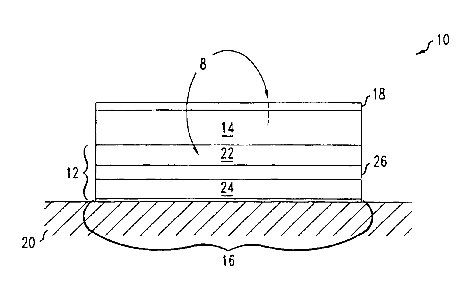
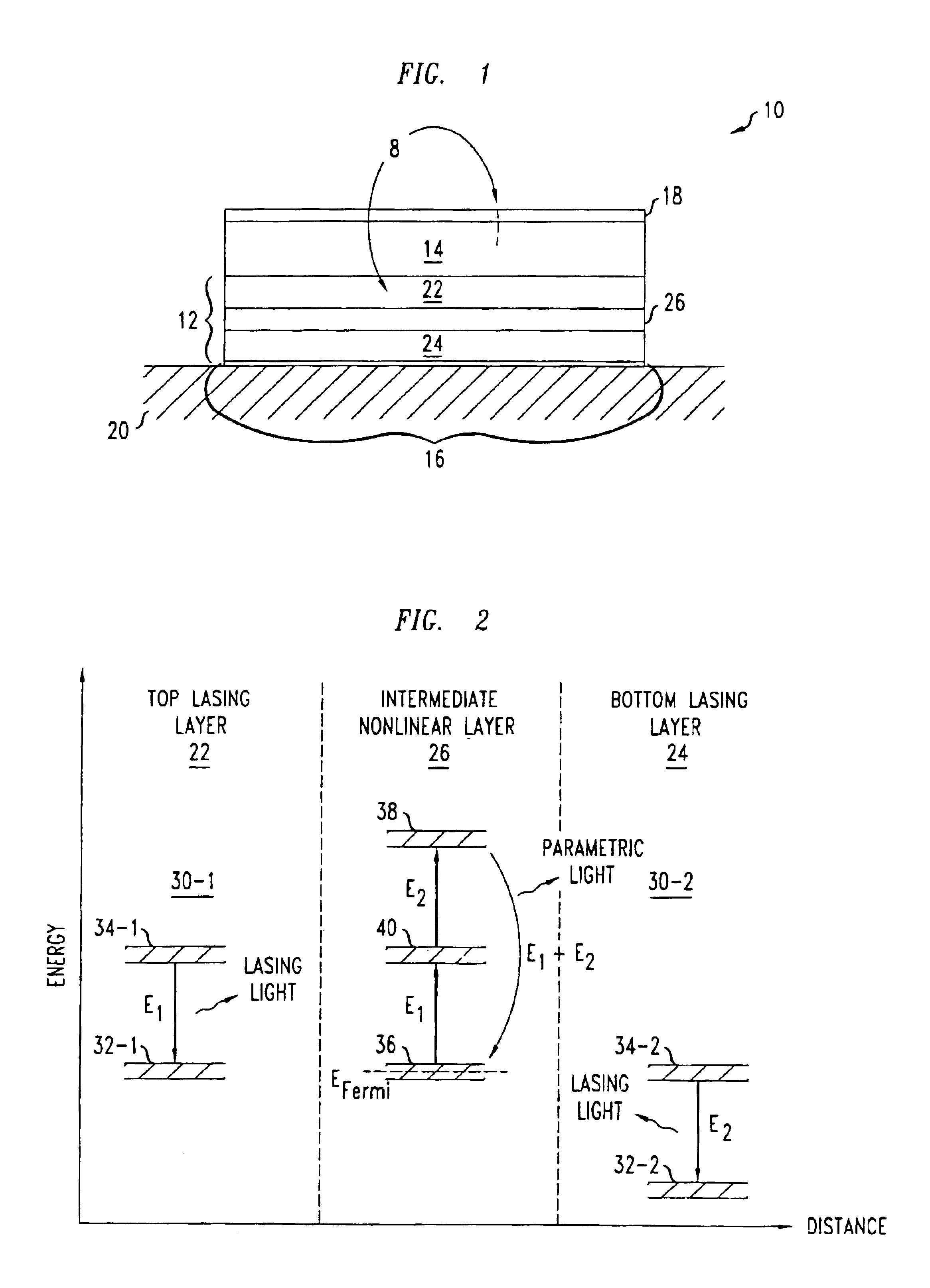
FIG. 1 shows an end view of one embodiment of a parametric light source 10. The parametric light source 10 has an optical laser cavity. The laser cavity includes an optical waveguide with an optical core layer 12 and top and bottom optical cladding layers 14, 16 and reflective and partially reflective end facets 8 at the ends of the cavity. The optical core layer 12 functions as an active layer for producing both stimulated emission light and parametric light. The stimulated emission light results from pumping the optical core layer 12 with a current via metallic electrode 18 and a conductive substrate 20. The stimulated emission or laser light produces parametric light via two-photon processes in the nonlinear optical medium of the optical core layer 12.

In the optical core layer 12, top and bottom lasing layers 22, 24 are the sources of the laser light and an intermediate nonlinear optical layer 26 includes the...


PUM

PropertyMeasurementUnit
lasing wavelengthsaaaaaaaaaa
heightaaaaaaaaaa

Abstract

A monolithic apparatus has a laser optical cavity. The laser optical cavity has a multi-layer structure that includes a first active semiconductor multi-layer and a second semiconductor multi-layer. The second semiconductor multi-layer is located laterally adjacent to the first active semiconductor multi-layer. The first active semiconductor multi-layer includes a sequence of quantum well structures that produce light of a lasing frequency in response to being electrically pumped. The second semiconductor multi-layer includes a sequence of quantum well structures and is configured to both absorb light of the lasing frequency and produce one of parametric light and harmonic light in response to absorbing light of the lasing frequency.

Description

1. Field of the InventionThe invention relates to semiconductor light sources and semiconductor lasers.2. Discussion of the Related ArtMaterials with large second-order and / or third-order nonlinear susceptibilities can produce direct optical frequency-conversion. In direct optical frequency-conversion, incident light generates new light with a frequency that is the sum, difference, or a harmonic of the frequency or frequencies of the incident light. Thus, incident light at frequencies .omega..sub.1 and .omega..sub.2 produces light at one or more of the frequencies .omega..sub.1 +.omega..sub.2, .omega..sub.1 -.omega..sub.2, 2.omega..sub.1, 2.omega..sub.2, 3.omega..sub.1, 3.omega..sub.2, etc. Herein, the light produced by nonlinear processes at sums and differences of incident frequencies will be referred to as parametric light, and the light produced by nonlinear processes at doubles, triples, etc. of an incident frequency will be referred to as harmonic light.Nonlinear optical mater...

Claims


Application Information

Patent Timeline
Patent Type & Authority Patents(United States)
IPC IPC(8): H01S3/13H01S3/08H01S3/10H01S5/00G02F1/39H01S5/06H01S5/32H01S5/34
CPCB82Y20/00H01S5/0604H01S5/3402G02F1/39H01S3/1083H01S3/109H01S5/3425H01S5/305H01S5/3054H01S5/3211H01S5/3213H01S5/0605
Inventor CAPASSO, FEDERICOCHO, ALFRED YICOLOMBELLI, RAFFAELEGMACHL, CLAIRE FOWSCHIMIKOW, NINASIVCO, DEBORAH LEE
Owner ALCATEL-LUCENT USA INC
Why Eureka
Try Eureka