Semiconductor structure and forming method thereof

A technology of semiconductor and gate structure, which is applied in the field of semiconductor structure and its formation, can solve the problems of semiconductor structure reliability to be improved, and achieve the effect of reducing the risk of short circuit, reducing the impact, and improving the etching selectivity

Pending Publication Date: 2022-05-03
SEMICON MFG INT (SHANGHAI) CORP +1
View PDF0 Cites 0 Cited by
  • Summary
  • Abstract
  • Description
  • Claims
  • Application Information

AI Technical Summary

Problems solved by technology

[0003] However, the reliability of existing semiconductor structures still needs to be improved

Method used


Image

  • Semiconductor structure and forming method thereof
  • Semiconductor structure and forming method thereof
  • Semiconductor structure and forming method thereof

Examples


Embodiment Construction

[0041]As mentioned in the background, the reliability of existing semiconductor structures still needs to be improved.

[0042] The reason why the reliability of the semiconductor structure still needs to be improved will be described in detail below with reference to the accompanying drawings.

[0043] Figure 1 to Figure 3 It is a structural schematic diagram of each step of a method for forming a semiconductor structure.

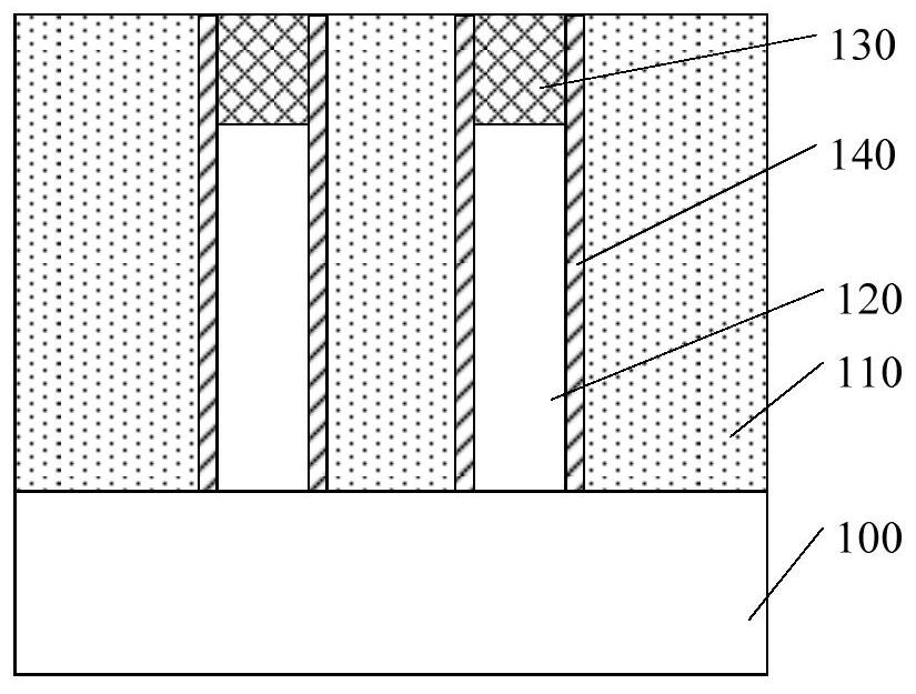
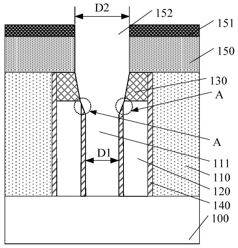
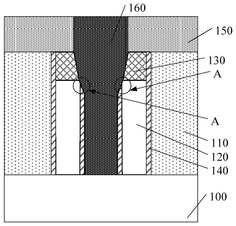
[0044] Please refer to figure 1 , providing a substrate 100, the substrate 100 includes a substrate (not shown), and a plurality of fin structures (not shown) located on the substrate separated from each other; a first dielectric layer (not shown) is formed on the surface of the substrate 100 shown), the first dielectric layer covers part of the side wall of the fin structure.

[0045] Please continue to refer figure 1 , forming a second dielectric layer 110 on the surface of the first dielectric layer, the second dielectric layer 110 has a plurality...


PUM


Abstract

The invention discloses a semiconductor structure and a forming method thereof. A first dielectric layer, a plurality of gate structures located in the first dielectric layer and side walls located on the side wall faces of the gate structures are formed on the substrate, source and drain structures are formed in the portions, on the two sides of the gate structures, of the substrate, and the first dielectric layer is further located on the surfaces of the source and drain structures; the side wall comprises a first area and a second area located on the first area; after the side walls are formed, the first dielectric layer is etched, a plurality of conductive openings are formed in the first dielectric layer, the conductive openings are exposed out of the surface of the source-drain structure, and in the process of etching the first dielectric layer, the etching rate of the side walls of the second region is smaller than that of the side walls of the first region; and forming a conductive structure in the conductive opening. Therefore, the reliability of the semiconductor structure is improved.

Description

technical field [0001] The invention relates to the technical field of semiconductor manufacturing, in particular to a semiconductor structure and a forming method thereof. Background technique [0002] With the rapid development of integrated circuit manufacturing technology, the size of semiconductor devices in the integrated circuit is continuously reduced, so that the operation speed of the entire integrated circuit will be effectively improved. As the size of components is required to be smaller and smaller, correspondingly, the size of the formed conductive structure connected to the semiconductor device is smaller and smaller. [0003] However, the reliability of existing semiconductor structures still needs to be improved. Contents of the invention [0004] The technical problem solved by the present invention is to provide a semiconductor structure and its forming method, so as to improve the reliability of the formed semiconductor structure. [0005] In order t...

Claims


Application Information

Patent Timeline
Patent Type & Authority Applications(China)
IPC IPC(8): H01L29/78H01L29/423H01L21/336
CPCH01L29/66803H01L29/785H01L29/42356
Inventor 郑二虎李凤美郑春生
Owner SEMICON MFG INT (SHANGHAI) CORP
Why Eureka
Try Eureka