Low dark count rate semiconductor structure
A technology of photosensitive semiconductor and shielding structure, which is applied in the direction of semiconductor devices, sustainable manufacturing/processing, climate sustainability, etc. It can solve the problems that it is difficult to determine the real DCR of ordinary photodiodes and become negative
- Summary
- Abstract
- Description
- Claims
- Application Information
AI Technical Summary
Problems solved by technology
Method used
Image
Examples
Embodiment Construction
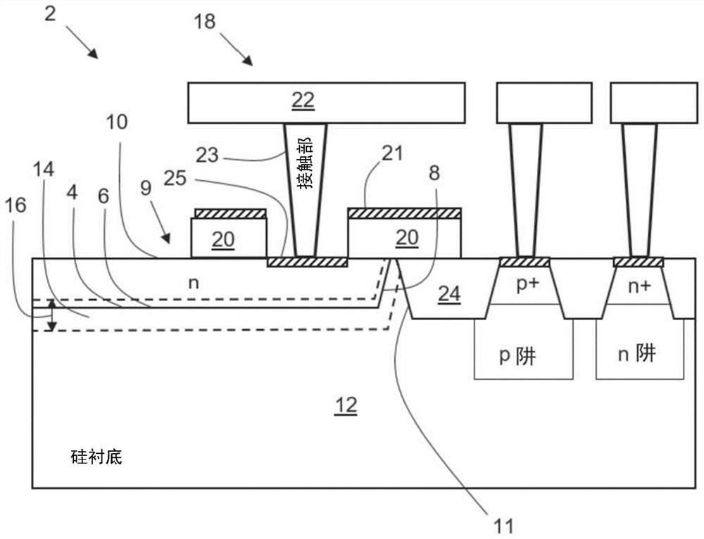
[0010] One source of higher DCR is surface damage to the silicon by the plasma process during fabrication. For DCR, the most vulnerable parts of SPAD or APD are the multiplication and depletion regions around the pn junction. Therefore, the portion of the pn junction closest to the silicon surface (ie, the edge of the pn junction) is critical for improving DCR. Metal and to some extent polycrystalline (polysilicon) on or above the silicon surface shield the energetic particles of the plasma from the surface, but surface damage can still occur which increases the DCR.
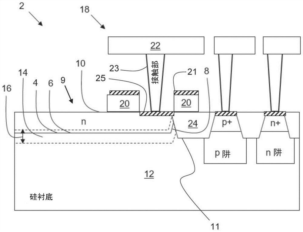
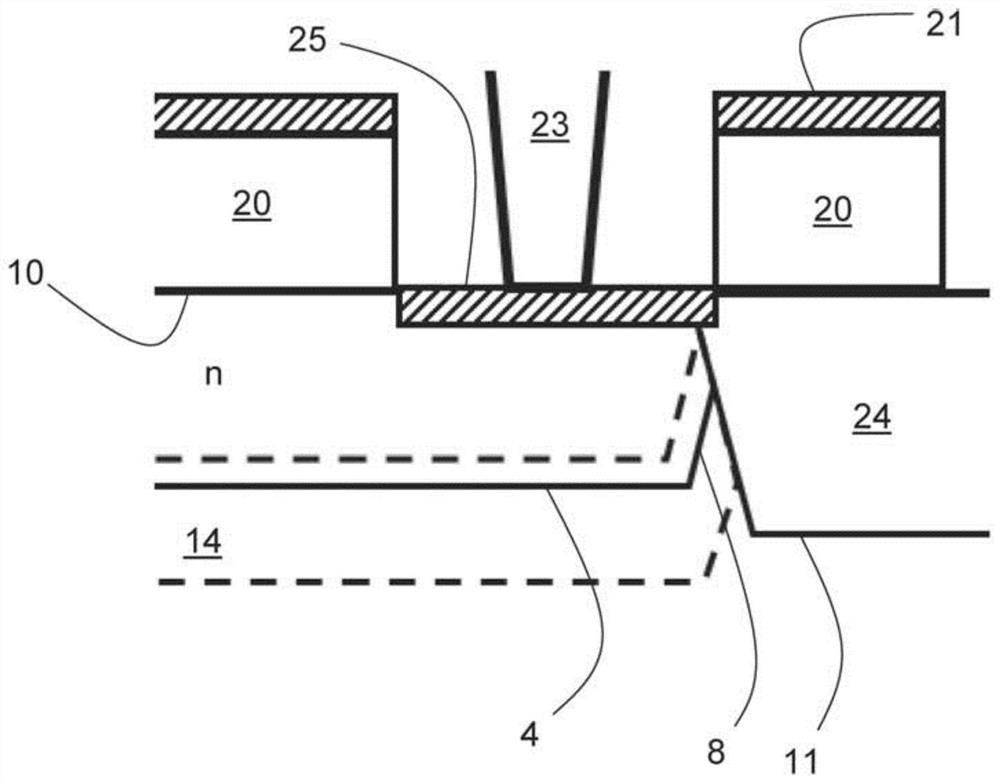
[0011] figure 1 A schematic cross-section of a part of a semiconductor structure 2 , eg in a SPAD or APD, is shown. The semiconductor structure comprises a pn junction 4 having a central portion 6 and an edge portion 8 surrounding the central portion 6 . The central part 6 of the pn junction is usually rectangular (eg square), but may also have other shapes, eg circular. The edge portion 8 is the portion of ...
PUM
 Abstract
Description
Claims
Application Information


