

5G precision circuit board back drilling hole depth control method
A technology of drilling depth and back-drilling, which is used in printed circuits, multilayer circuit manufacturing, printed circuit manufacturing, etc., can solve problems such as affecting product progress and delivery time, wasting time, and costing more, so as to reduce scratches risk, reduce online time, save time
- Summary
- Abstract
- Description
- Claims
- Application Information
AI Technical Summary
Problems solved by technology
Method used
Image

Examples
Embodiment
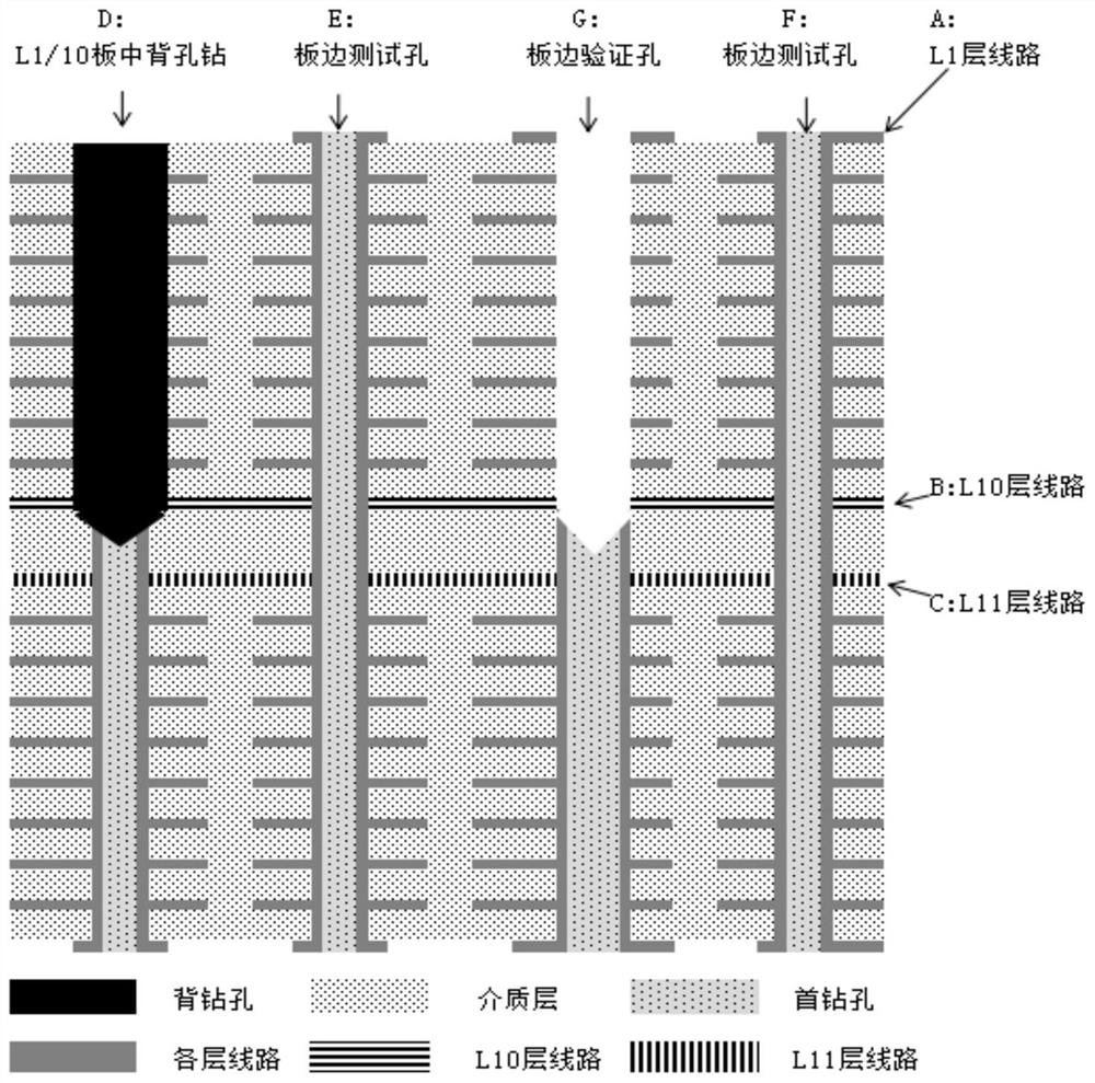
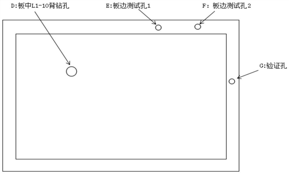
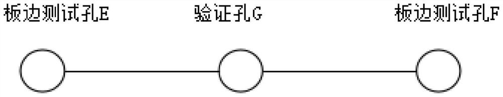
[0036] A 5G precision circuit board back drilling depth control method, such as Figure 1-2 , the method is: open a board edge test hole E, a board edge test hole F and at least one verification hole G on the edge of the laminated circuit board, and pass the detection of the verification hole G and the board edge test hole E and / or the board edge test hole The conduction state of F is used to control the back-drilled hole D on the circuit board to reach the required depth. The depth requirement of the back-drilled hole D is between the 10th and 11th layers of the circuit board. Again, figure 2 The inner frame is the required PCB that is installed on the equipment and facilities after processing and other measures; the outer frame is an auxiliary part added to complete the PCB processing, and the outer frame will be recycled as waste after the PCB is formed. The method includes the following steps:
[0037] (1) Drill through at least three positions on the edge of the laminat...
PUM
 Abstract
Description
Claims
Application Information