Frequency domain enhancement for efficient detection of low SNR flattened residue/stain defects

A defect and flat technology, applied in the field of detection of large residue and stain defects, can solve problems such as increasing the difficulty of detection

Pending Publication Date: 2022-05-13
KLA TENCOR CORP
View PDF0 Cites 0 Cited by
  • Summary
  • Abstract
  • Description
  • Claims
  • Application Information

AI Technical Summary

Problems solved by technology

[0006] However, defects such as residue or smudges (i.e., flat pattern defects) scattered in a noisy background and visible at image level are difficult to detect using conventional algorithms
When analyzing flat pattern defects, pixel-level differences are often hidden in the noise floor, which increases Detection difficulty
Furthermore, it is difficult to detect defects in wafer images with straight or wavy line patterns at low noise rates, especially with conventional single die technology

Method used


Image

  • Frequency domain enhancement for efficient detection of low SNR flattened residue/stain defects
  • Frequency domain enhancement for efficient detection of low SNR flattened residue/stain defects
  • Frequency domain enhancement for efficient detection of low SNR flattened residue/stain defects

Examples


Embodiment Construction

[0019] The disclosure has been particularly shown and described with respect to certain embodiments and specific features thereof. The embodiments set forth herein are to be regarded as illustrative and not restrictive. It will be apparent to those skilled in the art that various changes and modifications in form and details can be made without departing from the spirit and scope of the present disclosure. Reference will now be made in detail to the disclosed subject matter which is illustrated in the accompanying drawings.

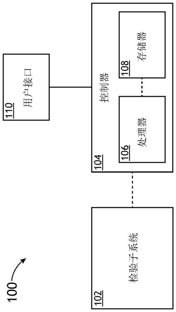
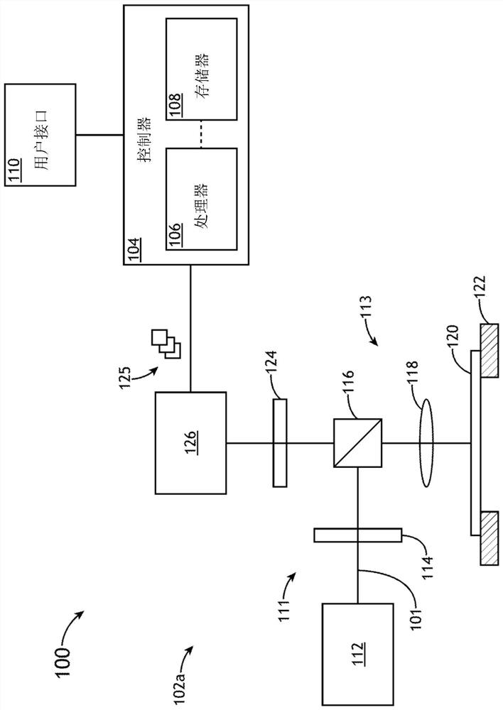
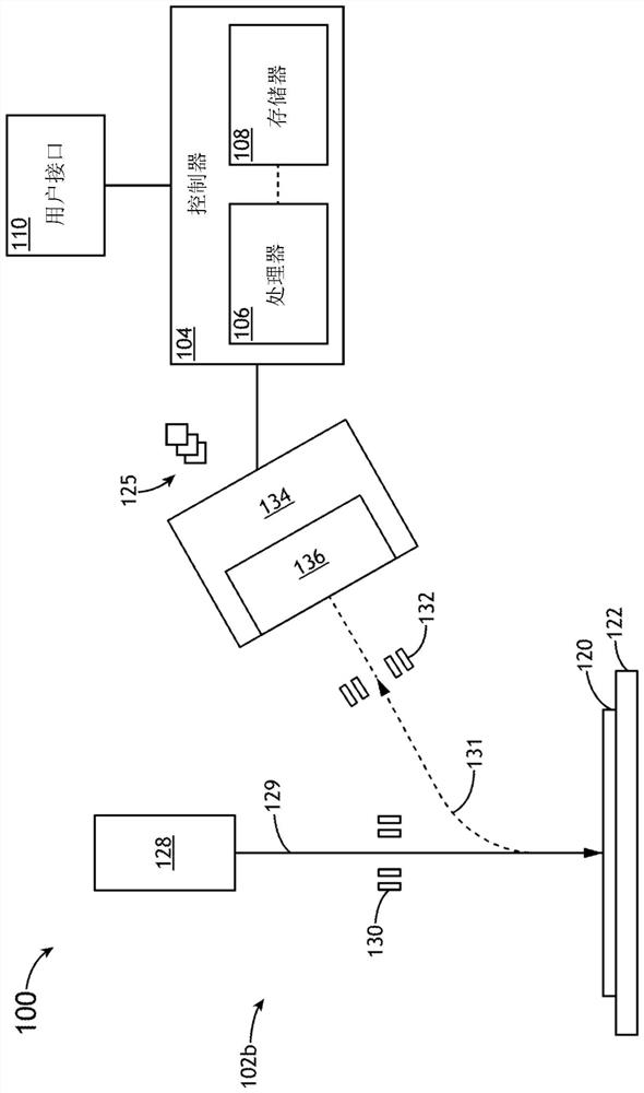
[0020] Embodiments of the present disclosure relate to an inspection system and method. The inspection system can be configured to detect one or more defects on a sample (eg, a semiconductor wafer or a photomask). The system may entail illuminating a sample with photons or electrons and receiving the illumination (eg, photons or electrons reflected and / or scattered from the sample) at one or more detectors to generate image data.

[0021] Image data ma...


PUM


Abstract

The invention discloses an inspection system. The system includes a controller communicatively coupleable with an inspection subsystem configured to receive illumination from a sample and generate image data. The controller includes one or more processors configured to execute program instructions to cause the one or more processors to: receive the image data, where the image data includes at least one image; performing downsampling on the at least one image by using bicubic interpolation or bilinear interpolation; transforming the at least one image from a spatial domain to a frequency domain using Fourier transform; filtering frequencies above a threshold frequency from the at least one image; transforming the at least one image from the frequency domain to the spatial domain using an inverse Fourier transform; and detecting one or more flat pattern defects in the at least one image.

Description

[0001] Cross References to Related Applications [0002] This application asserts an application filed on October 2, 2019 under 35 U.S.C. § 119(e) entitled "FREQUENCY DOMAIN ENHANCEMENT OFLOW-SNR FLAT RESIDUES / STAINS DEFECT FOR EFFECTIVE DETECTION), U.S. Provisional Application No. 62 / 909,582, in which Chaohong Wu and Yong Zhang are inventors, which is incorporated herein by reference in its entirety. technical field [0003] The present disclosure relates generally to the detection of defects in semiconductor wafers and photomasks, and in particular to the detection of large residue and smudge defects on wafer die. Background technique [0004] In conventional systems for detecting defects on a sample (eg, a semiconductor wafer or photomask), an illumination source illuminates the sample and a detector (eg, a camera) receives the illumination reflected or scattered from the sample. The detector produces image data, which is then transmitted to a computer system. The imag...

Claims


Application Information

Patent Timeline
IPC IPC(8): G06T7/00G06T7/37
CPCG06T7/0006G06T7/0004G06T7/37G06T2207/10061G06T2207/30148G06T2207/20056G06T5/20G06T3/40
Inventor 巫朝红永·张
Owner KLA TENCOR CORP
Why Eureka
Try Eureka