Display panel and display panel manufacturing method

A technology for a display panel and a manufacturing method, which is applied to semiconductor devices, electrical components, circuits, etc., can solve problems such as cross-coloring, and achieve the effects of low cost, good display effect, and improved product brightness.

Pending Publication Date: 2022-05-31
CHUZHOU HKC OPTOELECTRONICS TECH CO LTD +1
View PDF0 Cites 2 Cited by
  • Summary
  • Abstract
  • Description
  • Claims
  • Application Information

AI Technical Summary

Problems solved by technology

[0003] This application provides a display panel and a method for manufacturing a display panel, including but not limited to solving the problem of cross-color

Method used


Image

  • Display panel and display panel manufacturing method
  • Display panel and display panel manufacturing method
  • Display panel and display panel manufacturing method

Examples


Embodiment 1

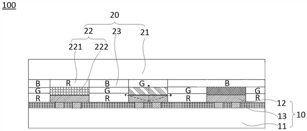
[0046] Embodiment 1 of the first aspect of the present application proposes a display panel. Please refer to figure 1 , the display panel 100 includes an array substrate 10 and a color filter substrate 20 disposed opposite to each other.

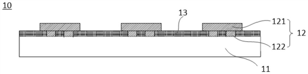
[0047]The array substrate 10 includes a first substrate 11 and a plurality of micro LEDs 12 , and the plurality of micro LEDs 12 are arrayed on the first substrate 11 at intervals. The micro-LED 12 refers to a micro-LED with a chip size between 0.5-200 microns. The micro-LED 12 can be a micro LED with a chip size between 0.5-100 microns, or a chip with a chip size between 50-200 microns. between miniLEDs. In this embodiment, the micro LED 12 is described as a micro LED.

[0048] A driving circuit (not shown) is also provided on the first substrate 11, and the driving circuit may include several scanning lines, several signal lines, and thin film transistors (Thin Film Transistor, TFT) arranged in an array, wherein the multiple scanning li...

Embodiment 2

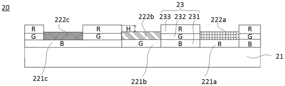
[0068] The display panel provided in the second embodiment is similar to that in the first embodiment, including a first substrate 11 and a second substrate 21 oppositely arranged, micro LEDs 12 arrayed on the first substrate 11, and a color conversion panel arranged on the second substrate 21 The light-shielding element 23 includes a first color-resist layer 231 , a second color-resist layer 232 and a third color-resist layer 233 stacked on the second substrate 21 in sequence.

[0069] Please refer to Figure 4 , Figure 4 It schematically shows the color filter substrate 20 in the display panel provided by the second embodiment, wherein the first color-resist layer 231 in the light-shielding member 23 is a blue color-resist layer, the second color-resist layer 232 is a red color-resist layer, and the third color-resist layer The resist layer 233 is a green color resist layer, that is, the stacking sequence of the color resist layers in the light shielding member 23 is B-R-G...

Embodiment 3

[0072] The display panel provided in the second embodiment is similar to that in the first embodiment, including a first substrate 11 and a second substrate 21 oppositely arranged, micro LEDs 12 arrayed on the first substrate 11, and a color conversion panel arranged on the second substrate 21 Device 22 and shade 23.

[0073] Please refer to Figure 5 , Figure 5 The color filter substrate 20 in the display panel provided by the third embodiment is schematically shown, wherein the light-shielding member 23 includes a first color-resist layer 231 and a second color-resist layer 232 stacked on the second substrate 21 in sequence, the first color-resistor Layer 231 is a blue color-resist layer, and the second color-resist layer 232 is a red color-resist layer.

[0074] In this embodiment, the shading member 23 includes both a blue color-resisting layer and a red color-resisting layer, so that the shading member 23 can play a role of shading light; and, the blue light emitted by...


PUM


Abstract

The invention is suitable for the technical field of display, and provides a display panel which comprises a first substrate and a second substrate which are oppositely arranged. The plurality of micro LEDs are arrayed on the first substrate at intervals; the plurality of color converters are arranged on the second substrate and are opposite to the micro LEDs respectively, each color converter comprises a color filter film and a quantum dot layer which are stacked, and the quantum dot layer is used for changing the wavelength of light; the shading part is located between the adjacent color converters, the shading part at least comprises a first color resistance layer and a second color resistance layer which are sequentially arranged on the second substrate in an overlapped mode and are different in color, and the shading part is right opposite to a gap between the adjacent micro LEDs. The invention further provides a manufacturing method of the display panel. According to the display panel and the display panel manufacturing method provided by the invention, color crossing between the sub-pixels can be effectively avoided, the manufacturing process is simple, and the cost is relatively low.

Description

technical field [0001] The present application belongs to the field of display technology, and in particular relates to a display panel and a method for manufacturing the display panel. Background technique [0002] Due to its performance advantages of high color saturation, quantum dot display has become the next generation of new display innovation technology. At present, display devices based on quantum dot materials usually include monochromatic micro LEDs or mini LEDs and quantum dot color conversion layers. With the development of technology, the chip size of micro LED or mini LED and the spacing between chips are getting smaller and smaller. In order to prevent color crossover between different sub-pixels, in the process of making the quantum dot color conversion layer, it is usually necessary to make Quantum dot barrier layer, however, the production of quantum dot barrier layer will add a yellow light process, the process is more cumbersome and the cost is higher. ...

Claims


Application Information

Patent Timeline
Patent Type & Authority Applications(China)
IPC IPC(8): H01L33/50H01L33/48H01L33/58H01L25/075H01L33/60
CPCH01L33/507H01L25/0753H01L33/48H01L33/58H01L33/60H01L2933/0033H01L2933/0058H01L2933/0041
Inventor 王然龙袁海江
Owner CHUZHOU HKC OPTOELECTRONICS TECH CO LTD
Why Eureka
Try Eureka