
Semiconductor element with decoupling unit and preparation method thereof

A semiconductor and decoupling technology, used in semiconductor/solid-state device manufacturing, semiconductor devices, and semiconductor/solid-state device components, etc., can solve the problems of increased number and complexity, and achieve the effect of improving reliability

Pending Publication Date: 2022-06-03
NAN YA TECH
View PDF0 Cites 0 Cited by
  • Summary
  • Abstract
  • Description
  • Claims
  • Application Information

AI Technical Summary

Problems solved by technology

However, during the process of shrinking dimensions, different problems are added, and such problems continue to increase in number and complexity
Therefore, there are still ongoing challenges in achieving improved quality, yield, performance and reliability, and reduced complexity

Method used


Image

  • Semiconductor element with decoupling unit and preparation method thereof
  • Semiconductor element with decoupling unit and preparation method thereof
  • Semiconductor element with decoupling unit and preparation method thereof

Examples


Embodiment Construction

[0159] Specific examples of components and configurations are described below to simplify embodiments of the present disclosure. Of course, these examples are for illustration only, and are not intended to limit the scope of the present disclosure. For example, in the description where the first part is formed on the second part, this may include embodiments where the first and second parts are in direct contact, and may also include additional parts formed between the first and second parts, Embodiments so that the first and second parts are not in direct contact. Additionally, embodiments of the present disclosure may repeat reference numerals and / or letters in many instances. These repetitions are for the purpose of simplicity and clarity, and do not in themselves represent a specific relationship between the various embodiments and / or the configurations discussed, unless the context specifically indicates otherwise.

[0160] Furthermore, for ease of description, spaces s...


PUM

PropertyMeasurementUnit
thicknessaaaaaaaaaa

Abstract

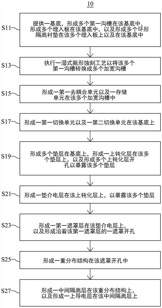
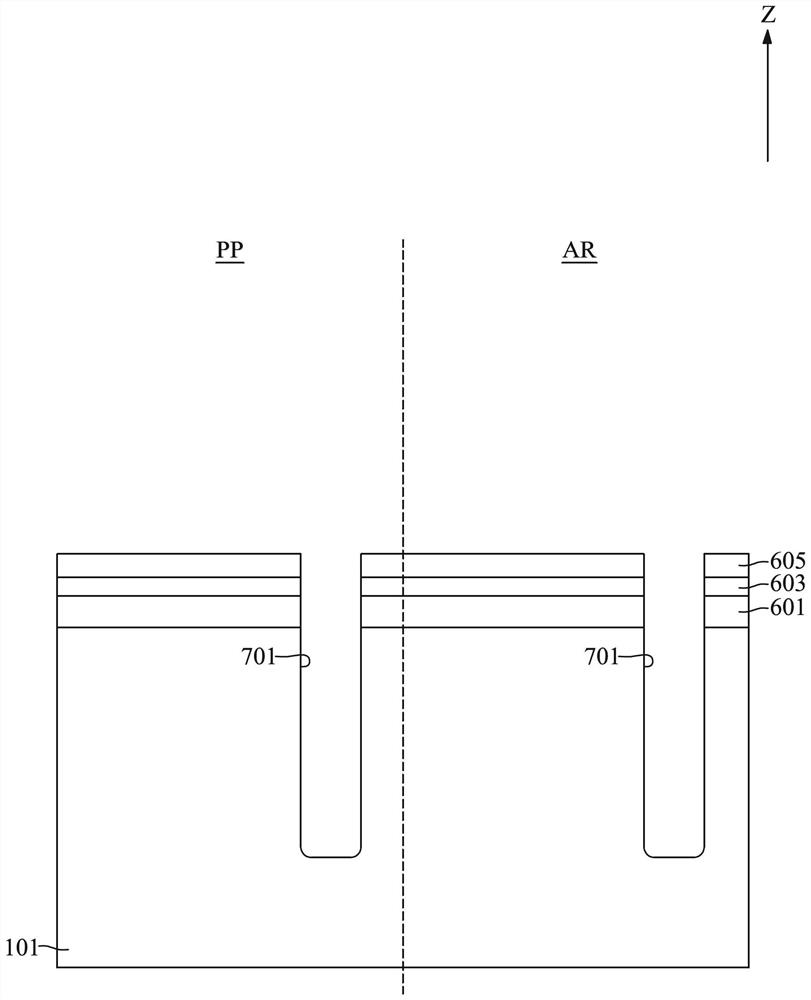
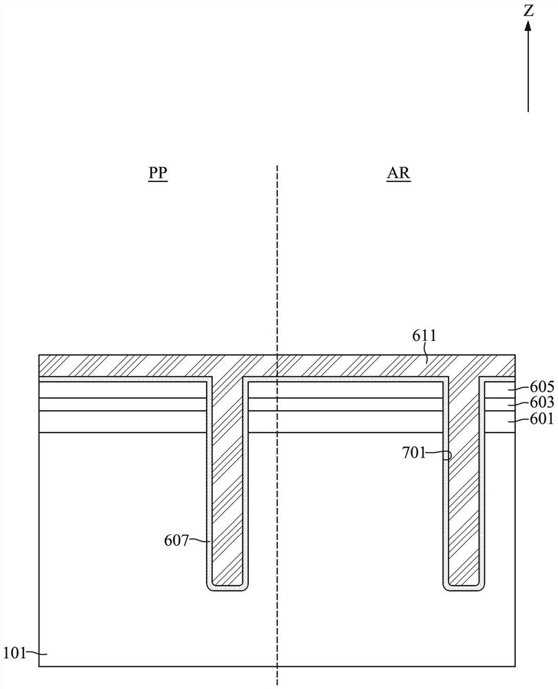
The invention provides a semiconductor element with a decoupling unit and a preparation method thereof. The semiconductor device has a substrate including an array region and a surrounding region disposed adjacent to the array region; a first decoupling unit located in the peripheral region of the substrate; a memory cell located in the array region of the substrate; a redistribution structure on the peripheral region and the array region of the substrate; an intermediate isolation layer on the redistribution structure in the peripheral region; and an upper conductive layer on the intermediate isolation layer. The redistribution structure on the peripheral region, the intermediate isolation layer, and the upper conductive layer together are configured as a second decoupling unit.

Description

[0001] cross reference [0002] The present disclosure claims priority to and the benefit of US Official Application Serial No. 17 / 108,736, filed on December 1, 2020, the contents of which are incorporated herein by reference in their entirety. technical field [0003] The present disclosure relates to a semiconductor element and a method for manufacturing the same. In particular, it relates to a semiconductor element with a decoupling unit and a manufacturing method thereof. Background technique [0004] Semiconductor components are used in different electronic applications such as personal computers, cell phones, digital cameras, or other electronic devices. The size of semiconductor devices is gradually decreasing to meet the increasing demands of computing power. However, during downsizing processes, different problems are added, and such problems continue to increase in number and complexity. Accordingly, challenges continue to be achieved in achieving improved qual...

Claims


Application Information

Patent Timeline
Patent Type & Authority Applications(China)
IPC IPC(8): H01L23/48H01L21/768H01L23/522H01L23/64
CPCH01L23/5223H01L23/642H01L21/76831H01L21/76877H01L21/76847H01L23/481H01L29/945H01L28/60H10B12/37H10B12/0385H10B12/0387H10B12/09H01L24/20H01L2224/211H01L24/19H01L2924/1205H01L23/13
Inventor 黄则尧施信益
Owner NAN YA TECH
Learn More