Stamp hole arrangement structure for PCB and corresponding PCB forming method
A forming method and technology of stamp holes, which are applied in the field of stamp holes, can solve problems such as unreasonable structure of bridge-connected stamp holes, protruding board edges of residual piles of connecting ribs, etc., and achieve better shape flatness
- Summary
- Abstract
- Description
- Claims
- Application Information
AI Technical Summary
Problems solved by technology
Method used
Image

Examples
Embodiment 1
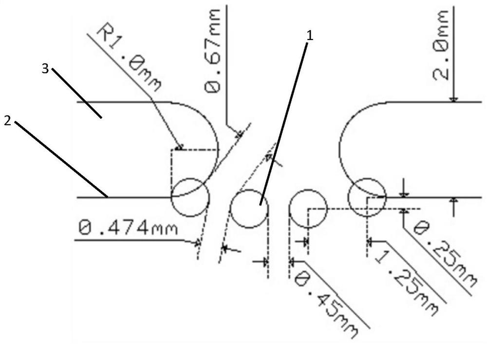
[0033] as attached figure 1 As shown in the figure, this embodiment is suitable for a small-sized conventional PCB, a kind of stamp hole arrangement structure for PCB, including four stamp holes 1 located in sequence near the current PCB outline, and two stamp holes located at the head and tail. 1 The center of the circle coincides with the outline 2 of the current PCB, and the two stamp holes 1 located in the middle are sunk by 0.25mm toward the inside of the PCB compared to the two stamp holes 1 located at the head and tail.
[0034] The groove-shaped PCB stamp hole is adopted, but the sinking distance in the middle will not cause the overall shape difference to be too large, which will lead to the splitting of the board. It avoids the problem of forming connecting rib residual piles after existing sub-slabs.
[0035] Four stamp holes 1 are used, the apertures of the four stamp holes 1 are all 0.8 mm, and the center-to-center distance of the adjacent stamp holes 1 is 1.1 mm...
Embodiment 2
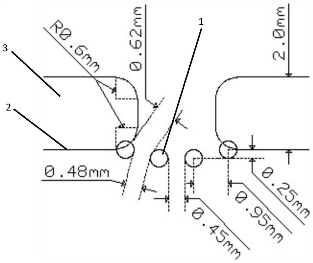
[0045] as attached figure 2 As shown, this embodiment is suitable for special situations such as small-sized optoelectronic boards and insufficient board edge space. A stamp hole arrangement structure for PCB includes four stamp holes 1 arranged in sequence near the current PCB outline 2, located in The centers of the two stamp holes 1 at the head and tail coincide with the outline 2 of the current PCB, and the two stamp holes 1 in the middle are sunk by 0.25mm toward the PCB compared to the two stamp holes 1 at the head and tail.
[0046] The groove-shaped PCB stamp hole is adopted, but the sinking distance in the middle will not cause the overall shape difference to be too large, which will lead to the splitting of the board. It avoids the problem of forming connecting rib residual piles after existing sub-slabs.
[0047] Four stamp holes 1 are used, the diameters of the four stamp holes 1 are all 0.5mm, and the center-to-center distance of the adjacent stamp holes 1 is 0....
Embodiment 3
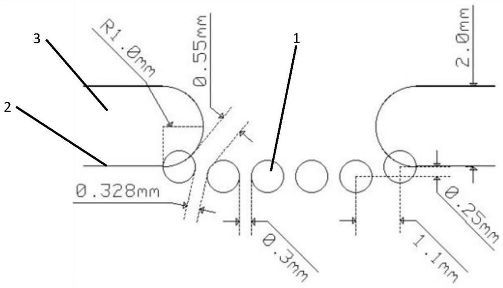
[0057] as attached image 3 As shown, this embodiment is suitable for a conventional PCB of general size, a stamp hole arrangement structure for PCB, including six stamp holes 1 located in sequence near the current PCB outline 2, and two stamp holes located at the head and tail. The center of the hole 1 coincides with the outline line 2 of the current PCB, and the four stamp holes 1 located in the middle are sunk by 0.25mm toward the inside of the PCB compared to the two stamp holes 1 located at the head and tail.
[0058] The groove-shaped PCB stamp hole is adopted, but the sinking distance in the middle will not cause the overall shape difference to be too large, which will lead to the splitting of the board. It avoids the problem of forming connecting rib residual piles after existing sub-slabs.
[0059] Six stamp holes 1 are used, the apertures of the six stamp holes 1 are all 0.8 mm, and the center-to-center distance of the adjacent stamp holes 1 is 1.1 mm.
[0060] A P...
PUM
 Abstract
Description
Claims
Application Information
 - R&D Engineer
- R&D Manager
- IP Professional
- Industry Leading Data Capabilities
- Powerful AI technology
- Patent DNA Extraction
Browse by: Latest US Patents, China's latest patents, Technical Efficacy Thesaurus, Application Domain, Technology Topic.
© 2024 PatSnap. All rights reserved.Legal|Privacy policy|Modern Slavery Act Transparency Statement|Sitemap