Image processing device

An image processing device and the technology of the processing device, which are applied in the direction of image communication, electrical recording technology using charge graphics, equipment using electrical recording technology using charge graphics, etc., can solve the problem of no circuit scale, unbalanced image up and down, left and right, and small unit data Deal with problems such as good methods to achieve the effect of preventing image tone from deteriorating

Inactive Publication Date: 2004-04-21
KK TOSHIBA
View PDF2 Cites 0 Cited by
  • Summary
  • Abstract
  • Description
  • Claims
  • Application Information

AI Technical Summary

Problems solved by technology

[0010] Also, because the compensation for this type of font is performed on the entire image, although it is effective for image quality degradation due to text fonts, it is still difficult to compensate for photos or half-tone image parts, especially when performing one-dimensional compensation. There is a problem of degradation of image tone
[0011] Furthermore, for the compensation of binary images, there is no small and good good method for multi-bit data processing.
[0012] As mentioned above, there are various compensation methods for image quality degradation caused by pixel distortion in imaging, but any of them is a one-dimensional compensation method, which cannot achieve sufficient effect on image quality degradation caused by text fonts. , only to compensate for the main scanning direction or only for the sub-scanning direction, there will still be problems of image imbalance
[0013] In addition, the above method of compensating for pixel distortion is performed on the entire image. Although this has a certain effect on the image quality degradation of the text part of the font, this compensation is performed on the photo or half-tone image part, especially for one-dimensional When compensating, there is a problem of image tone degradation
[0014] Furthermore, for the compensation of the binary image, there is no problem of an excellent method for performing unit data processing with a small circuit scale.

Method used


Image

  • Image processing device
  • Image processing device
  • Image processing device

Examples


Embodiment Construction

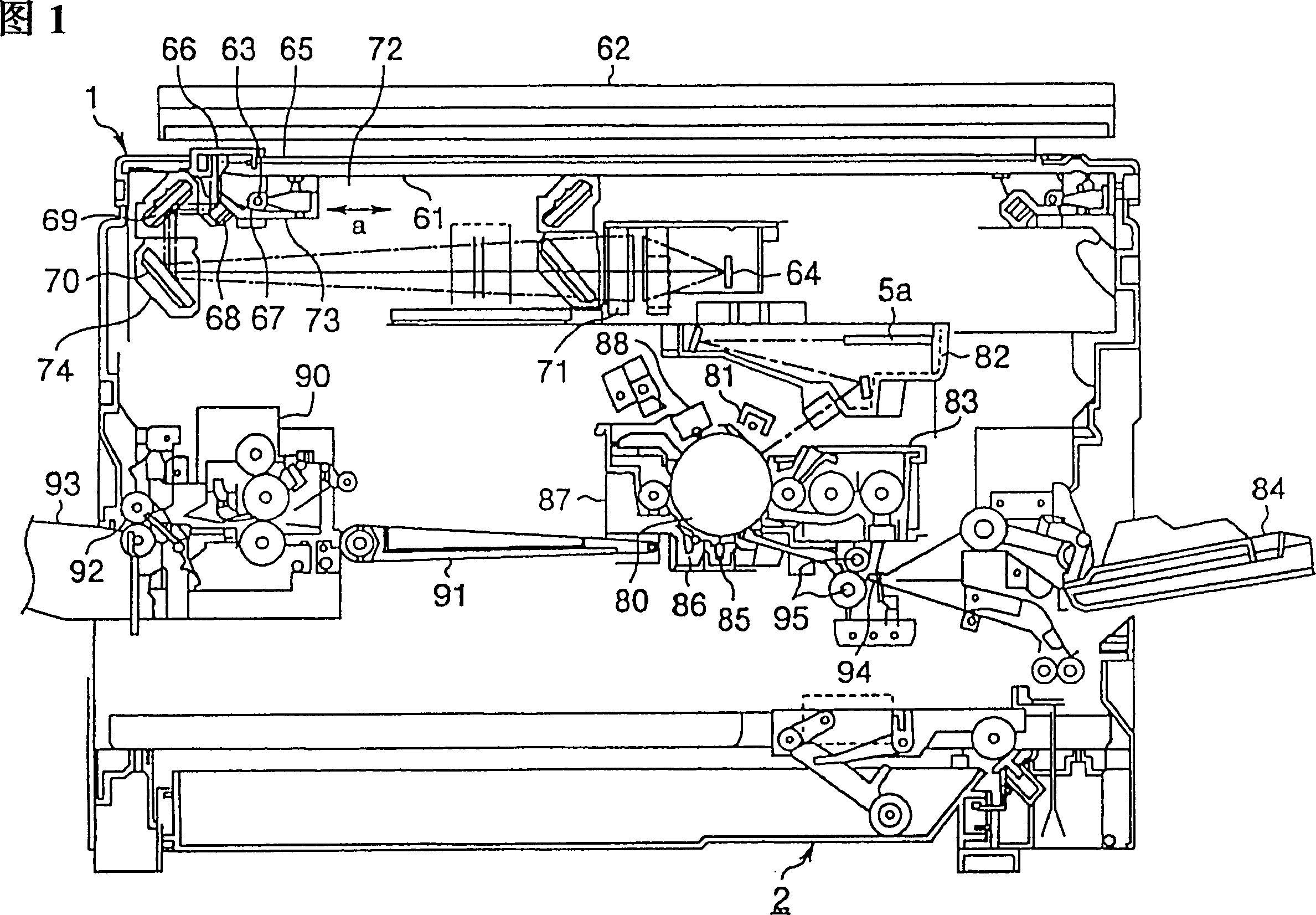
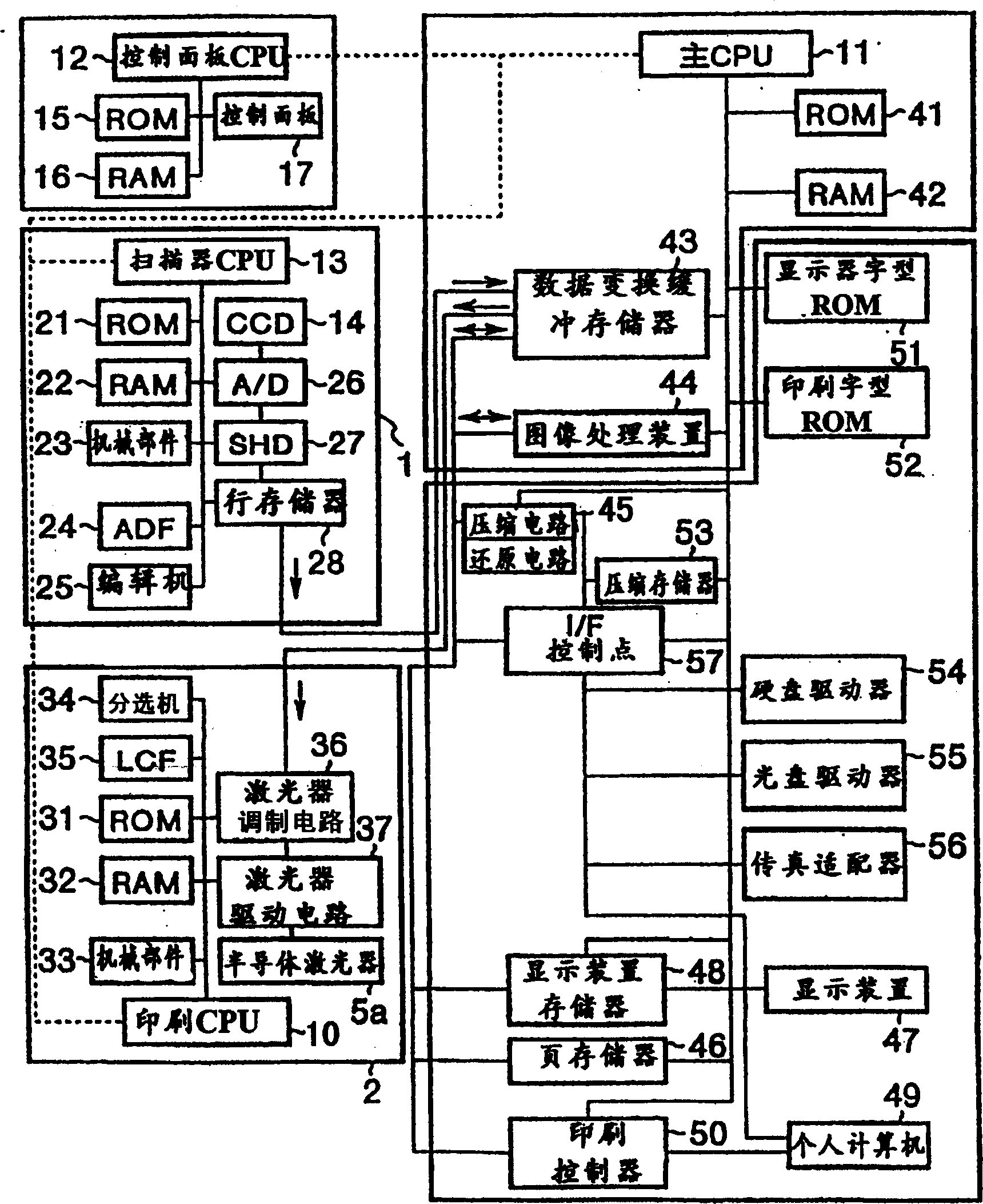
[0037] FIG. 1 shows a schematic configuration of a digital copier as an example of the image forming apparatus of the present invention. Specifically, this digital copying machine generally includes: a scanning unit 1 as a reading device for optically reading a document image; A printing section 2 as an image forming device that performs image forming on paper (media) by electrophotography.

[0038] The scanning part 1 has an original table 61 on which originals to be copied are loaded, a platen 62 that can press and hold the originals on the original table and can be opened and closed freely, a fluorescent lamp 63 installed on the original table 61 as a light source for illuminating the original, and a fluorescent lamp as a light source for illuminating the original. A CCD-type line sensor 64 of a photoelectric conversion device that performs photoelectric conversion of reflected light from the document after irradiation. In addition, the fluorescent lamp 63 is also equipped...


PUM


Abstract

To process an image while preventing image tone deterioration due to correction without losing the balance of the image and further excellently correcting the image with respect to the handling of multi-bit data. Inputted image data are sent to and processed by a high-picture- quality processing part 100 which performs a high-picture-quality processing by filtering, etc., and then sent to and enlarged or an enlargement / reduction processing part 101, and the data have gradations processed by a half-tone processing part 102 as desired and are corrected by a correction processing part 103 by pixels in two dimensions of the horizontal and vertical scanning directions, so that print data are outputted to a data switching / buffer memory 43.

Description

technical field [0001] The present invention relates to an image processing device and an imaging device having a function of storing image data obtained by reading an image in a memory, performing image processing on the stored image data to form an image on paper. Background technique [0002] There is such an imaging device, which uses a laser to scan the laser beam from a polygon mirror motor, so that the laser beam is irradiated on the photoreceptor, and the electrostatic latent image formed on it is developed by a developing device, and then recorded by a fixing device. An imaging device for imaging images on media. This technique has been widely used in laser printers, digital electronic copiers (PPC) and the like in recent years. [0003] When the above-mentioned laser is used to form an electrostatic latent image by turning on / off the image points one by one and develop it with fine toner, first, each image point must be made into a desired size. [0004] For exam...

Claims


Application Information

Patent Timeline
IPC IPC(8): G03G15/36H04N1/38H04N1/387H04N1/393H04N1/40H04N1/405
CPCH04N1/40093
Inventor 山西英一
Owner KK TOSHIBA
Why Eureka
Try Eureka